
Connections are obviously the lifeblood of electrical devices. PCB pads are the metallic surfaces that connect various PCB components in the board. Understanding them is crucial while manufacturing PCBs for an electrical device.
This blog will cover all the aspects related to them, including what is a PCB pad, what are they made of, types of pads, their function, and significance.
Key Highlights
- A PCB pad is the connecting point for electronic components on a PCB.
- PCB pads are normally made from copper as it has good conductivity. Tin and lead-based solder are more typical types of coatings which act as a thin layer between the copper and the outer surface of the conductor.
- Various types of PCB pads are: Through-hole pads, surface mount pads, Ball Grid Array (BGA) pad, solder mask defined pads, and non-solder mask defined pads.
- PCB pads are critically important during layout because they help in proper placement of components, acts as component leads, and improves signal integrity.
- PCB pads that act as vital connectors between component parts and the copper traces that make up the circuit paths.
What is a PCB pad?
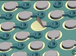
A PCB pad is the connecting point for electronic components on a PCB. These metallic surfaces make it easier to solder and attach components, as well as make electrical connections via copper traces. Pads are classified into many categories, the most popular of which being through-hole and surface mount pads.
Through-hole pads are holes drilled with metallic plating that allow components to be inserted and soldered from one side of the board to another. Components are directly soldered to flat surfaces of the board known as surface mount pads. Every variety has benefits, and the selection of a kind is contingent upon the particular demands of the manufacturing and circuit design procedures. This is especially important in designing multilayer PCB configurations where space and connectivity are optimised.
Proper pad design is critical for establishing stable electrical connections. Pad size, shape, and spacing have an influence on soldering quality and circuit performance. Well-designed pads increase production productivity and reduce the likelihood of faults, hence improving the lifetime and functioning of electronic devices.
What Are the Pads on a PCB Made Of?
PCB pads are normally made from copper as it has good conductivity and it is cheaper compared to other types of metal. Copper pads also offer a stable platform where some components can be soldered, and connections are established in the circuit. However, pure copper exposed to the environment undergoes oxidation and corrosion that affect the functionality of the PCB.
The copper pads also tend to have further layers of coatings to improve conductivity and to avoid corrosion. Tin and lead-based solder are more typical types of coatings which act as a thin layer between the copper and the outer surface of the conductor. These coatings enhance the solderability and provide enhanced bonding between the leads of the component and the pad. The application of ENIG (Electroless Nickel Immersion Gold) PCB coatings is common for protecting copper pads.
Types of PCB Pad
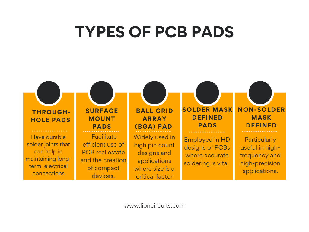
PCB pads are classified into through-hole pads that are used to install components with leads that go through drilled holes, surface mount pads that are used to solder components directly onto the PCB surface and Ball Grid Array (BGA) pads for BGA devices. These include Solder Mask Defined (SMD) and Non-Solder Mask Defined (NSMD) pads. Each type has its advantages depending on the application, such as single-sided PCB or complex multilayer PCB designs.
Through-hole Pad
It refers to an extended pad type by which through-hole components are mounted. These pads demand the placement of component pins through the vias. They have solid and durable solder joints that can help in maintaining long-term mechanical and electrical connections. However, they may limit the routing areas on multilayer boards by the component leads and the number of holes.
Surface Mount Pad
SMD pads are pads which are intended for use in surface mounting of the components. These pads enable the components to be soldered on the surface of the PCB without their leads passing through the holes. They offer advantages such as smaller footprint, higher component density, and easier automated assembly processes. Surface mount pads facilitate efficient use of PCB real estate and enable the creation of compact electronic devices.
Ball Grid Array (BGA) Pad
BGA pads are made specifically for BGA components where the bottom side is made of solder balls used to make contact with the PCB. BGA pads are a network of solder pads that make the electrical connection with the component used and the PCB. It can provide advantages of size reduction, increased electrical efficiency, and better thermal management. BGA pads are widely used in high pin count designs and applications where size is a critical factor. Advanced designs, such as HDI PCB (High-Density Interconnect), often utilise BGA technology for compact and efficient layouts.
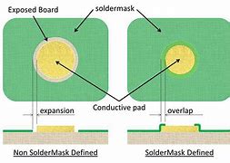
Solder Mask Defined Pads (SMD)
SMD pads lack copper for their definition and instead use a solder mask to outline the shape of the pad. This type of pad gives one full control over the soldering process right from the formation of the solder joints to stopping formation of solder bridges between the pads. SMD pads are often employed in HD designs of PCBs where accurate soldering is vital for the correct functionality of the device.
Non-Solder Mask Defined Pads (NSMD)
NSMD pads are different from those in which the solder paste area is contained by a solder mask, the area of an NSMD pad is open to the solder paste. This orientation offers advantages in terms of planarity and co-planarity and may enhance the connections for fine pitch devices. These pads are used when greater frequency, voltage or higher accuracy is required in the application or design. NSMD pads are particularly useful in high-frequency and high-precision applications like those found in ceramic PCB designs.
Function of Pads in PCB Design
Like any other PCB components, pads do play a crucial role in the functioning of a device. Check out some of the main functions:
- PCB pads are critically important during layout because they help in proper placement of components and their creation of interconnections.
- These small conductive zones help serve as contact points for component leads or solder to make electrical connections all over the board. It plays a critical role in determining the size and pitch of resistors, solder bridges, and tombstones in PCB assembly.
- Sufficient pad dimensions and distance helps to solder correctly without bridging between the pads or misplacing components.
- Pads play an essential role in signal integrity and thermal management of the desired substrate. It becomes essential for high-speed digital circuits that pads should not be the source of impedance discontinuities and signal reflections.
- Additionally, they aid in efficient heat dissipation from components, promoting thermal stability and preventing overheating-induced failures.
Role of Pads in PCB Layout
Undoubtedly, the placements of pads play a key role in the PCB layout. Here are some important points to note:
- Helps in Trace Routing: Pads may act as termination points for traces so that they can interconnect various components. Perfect pad placement reduce the need for longer traces and crosstalk between signals.Therefore, signal integrity may increase naturally.
- Avoids Tombstoning: in the case of surface mount placement, there are chances of tombstoning. It occurs when the PCB pads are lifted off by components due to irregular pad placements. As a result, the connection remains incomplete.
- Improves Component Placement: Usually, manufacturers place various PCB elements on the basis of parameters like circuit topology, high-speed paths, etc. By placing pads in a way that mirrors the logical flow of the circuit, the designer ensures that components are positioned optimally for electrical performance.
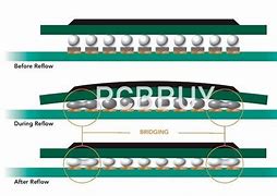
Prevents solder bridging: perfect placement of pads makes sure that proportions, reducing the risk of excess solder that can bridge between pads.
Significance of Pads in PCBs
PCB pads that act as vital connectors between component parts and the copper traces that make up the circuit paths. Their relevance stems from their critical role in guaranteeing the operation, reliability, manufacturability, and assembly of PCBs. Pads are needed for making secure electrical connections between components and traces. Their design has a direct influence on signal integrity and electrical performance. Properly constructed pads allow for more effective soldering, resulting in a strong connection that can survive environmental pressures and thermal cycling.
Pads have an impact on manufacturability because they affect the ease and precision with which components are placed during assembly procedures like pick and place. A well-designed pad layout makes assembly easier, reduces the possibility of mistakes, and increases overall production efficiency. Pad design is critical to preventing flaws and extending the life of the PCB. This eliminates the need for rework and improves the end product's reliability. In processes like PCB etching, precise pad design ensures clear and accurate circuit paths.
PCB Pad Sizes
It is very important to identify the appropriate pad sizes for the various components since it would influence the soldering and the electrical connections throughout the PCB. The guidelines can be originated based on, for example, the lead size of its component, type of its package, or the application it will be used for. Here are some general guidelines:
- Typically, more extensive components desire more extensive pads to ensure that leads are adequately covered while smaller components may cause solder bridging if they are provided with large pads.
- It is imperative to stay adherent to follow standard industry rules and regulation as well as the manufacturer guidelines.
- These standards, for example IPC standards, outline suggested pad sizes in relation to the component outline, spacing between leads, and soldering techniques employed.
- Manufacturers’ specifications are useful in giving more refined information on certain component details, including compatibility and performance.
Final Thoughts
PCB pads are essential interconnecting areas I/O points for the soldering of components and to mount them on the printed circuit board. There are through-hole and surface mount pads and each type has their benefits depending on the circuit design. The pads are generally of copper with overlaying coatings of the min, Pb-based solder, or gold for optimised conductivity and decreased corrosion. There are many kinds of pads, for example BGA pads that suit the kind of component that is to be mounted.
The pad design plays a significant role in making electrical connections dependable for soldering, signal interference, and heat dissipation. High-quality pads aid in the enhancement of manufacturing processes, decrease the rate of defects and also help in increasing the lifespan of the gadgets. It is crucial to be cognizant of pad sizes and legal requirements for designing PCBs and following the measurements recommended by the manufacturers.
%20(1).jpg)
