
Ever wondered how those tiny and intricate circuits are made on daily gadgets? Well, the answer lies in the process of PCB etching. It is the process of removing copper elements from the board to pave a conductive path for electricity flow.
Without the proper knowledge of what is PCB etching and its standards, manufacturers may find themselves struggling with various approaches during the process. This blog will cover every aspect of PCB etching, including the steps for the process, real-world examples, and types of etching.
Key Highlights
- PCB etching refers to the task of eliminating unwanted copper from the board surface.
- Manufacturers must prepare a design, transfer it, apply the etching solution, clean it, and perform a finishing process to etch PCB for an electrical device.
- Two common types of PCB etching are chemical etching and laser etching. Chemical etching is the process of immersing the PCB in a chemical solution but it is a cheaper solution while laser etching is an environment-friendly technique with a higher cost.
- Wet etching is the process of immersing the PCB in a chemical solution to wipe out unwanted copper from the surface while dry etching is the type of copper removal technique that uses gases or plasma.
- Manufacturers must clean the PCB surface, use high-quality copper clad laminates, give proper safety gear for workers, and mix the etching solution with baking soda for a smoother etching process.
What is PCB etching?
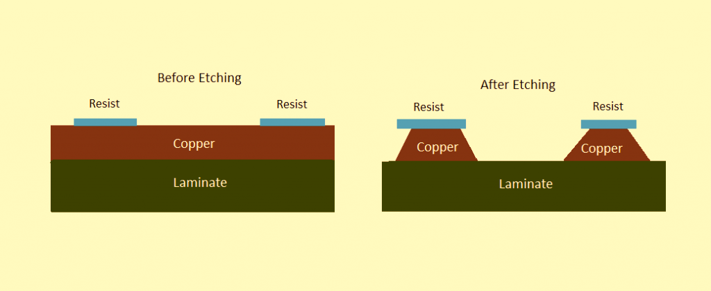
PCB etching refers to the task of eliminating unwanted copper from the board surface. Manufacturers can create desired circuit patterns only with the removal of unwanted copper traces through PCB etching. It is one of the most crucial steps after the PCB fabrication process.
Before starting with PCB etching, a process called photolithography is conducted to transfer the desired blueprint of the board. With the help of this layout, unwanted copper elements are traced out and removed. This is just the tip of the iceberg. There are many other techniques for the PCB etching process like chemical etching, laser etching, etc.
How to Etch PCB - Step-by-Step Guide
Considering the importance, PCB etching goes through a series of well-structured steps. Here is a detailed, step-by-step guide on how to etch a PCB:
1. Designing the PCB
First of all, a basic layout of the software is designed using various software like EAGLE, KiCad, or Altium Designer. The PCB components and connections of the PCB must be clearly laid out in the design with proper spacing. Verify that the PCB pad sizes and orientations match the component's PCB design constraints.
After designing, pick the transparency sheet to which you want to transfer the PCB design. You can transfer either through a laser or inkjet printer. Make sure that it is designed in the reverse format.
2. Transferring the Design
Clean the copper-clad board using fine sandpaper. Then, cut out the design perfectly to match it with the copper-clad board. Apply sufficient heat and pressure to ensure that the ink sticks to the copper surface firmly.
After the heating process, cool it down to peel off the transfer paper. Now, only the design will remain stuck to the copper surface.
3. Applying the etching solution
Most probably, manufacturers use ferric chloride, ammonium persulfate, or vinegar and hydrogen peroxide, as the etching solution. Choose one of them after considering factors like wire density, disposal, etc., and fill a tray with the solution.
Immerse the board in the solution and stir it. Ensure that you have trained professionals with proper safety gear to periodically verify whether the etching process is completed.
4. Clean the PCB
Clean the PCB after the etching process only under running water. Consider using a soft brush to scrub and remove any leftover copper from the surface. After cleaning, dry it with a clean cloth. It is recommended to do the entire cleaning process in a well-ventilated space to prevent inhaling fumes from the etching solution.
5. Finishing Process
PCB passes through many well-executed steps to complete the finishing process. Here is a breakdown:
i) In order to protect the remaining copper traces from oxidation, a thin layer of tin is applied to the surface.
ii) To prevent solder from bridging between adjacent copper traces, a solder mask is applied.
iii)Silkscreen printing is performed to label the board with the registration number, brand name, etc.
Types of PCB Etching
There are various types of PCB etching. Two of the most common types are:

1. Chemical Etching
Chemical etching is the process of immersing the PCB in a chemical solution like ferric chloride to dissolve away the unwanted copper. A resist material is applied before the process to protect the required copper traces. Manufacturers must make sure that the photoresists securely bond to the metal surface.
Advantages
- Chemical etching is comparatively a less expensive method as compared to other alternatives.
- Manufacturers can choose from a wide range of materials as most of them are compatible with chemical etching.
- Downtime is reduced because chemical etching components are easier to clean.
- It can be performed in a normal environment without any specialised equipment.
Disadvantages
- Chemical etching may not be effective for etching traces with dimensions less than 1μm.
- The process of chemical etching involves the usage of many chemical solutions. Disposal of wastes after the etching process would be a big problem.
- Direct exposure to some materials, especially the fumes arising in the process, poses health risks to the labourers.
- In chemical etching, there is an extra step of removing the tin layer from the board.
2. Laser Etching
In the laser etching process, the PCB is subjected to high-powered laser lines to create trace lines on the substrate surface. Then, these unwanted copper lines evaporate away. Well-trained manual labourers must constantly monitor throughout the process to detect any variations.
Advantages
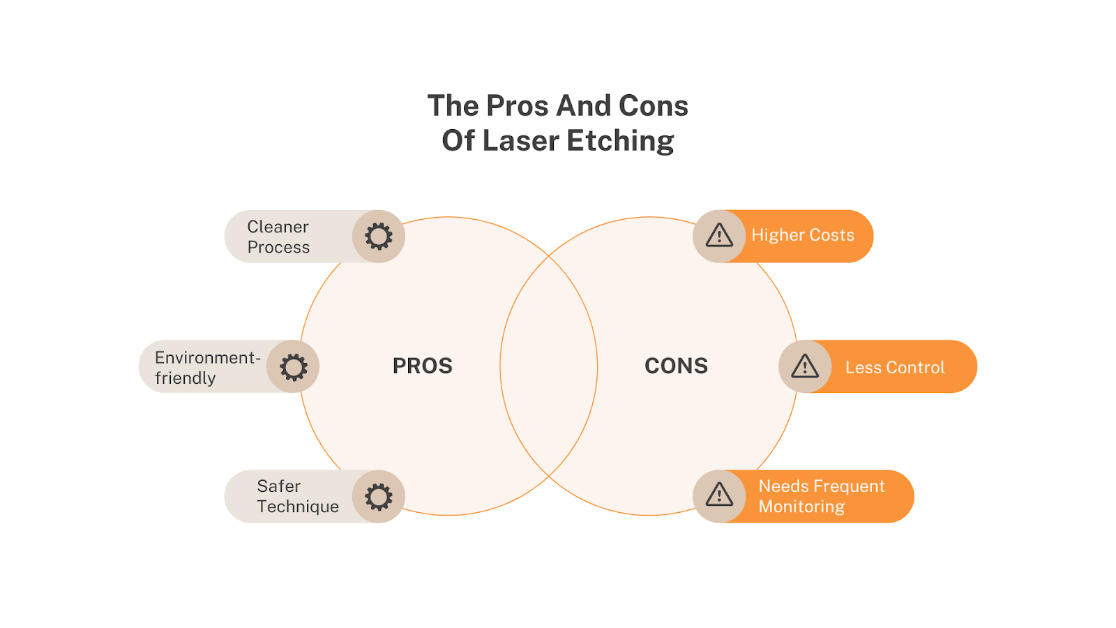
- Laser etching is more suitable for complex circuits as it is known for its high level of precision in intricate designs.
- Apart from chemical etching, laser etching is a cleaner process as it leaves no waste.
- Laser etching is considered an environment-friendly technique as it does not require any chemical substances.
- In laser etching, labourers are comparatively safer as no hazardous substances are involved.
Disadvantages
- Several specialised equipment are required for the process, which may lead to increased production costs.
- It is difficult to control the depth of the etching process because the shininess of the PCB surface can cause reflection issues.
- Labourers must frequently monitor the process.
- Even though hazardous chemicals are not involved, toxic fumes are generated in laser etching. Labourers must wear proper safety gear to protect from exposure.
Difference Between Wet Etching and Dry Etching
As the process of PCB etching gets complex, manufacturers try out more methods to simplify the procedure. Have a look at a comparison between the top two methods of PCB etching- wet etching and dry etching.
1. Meaning
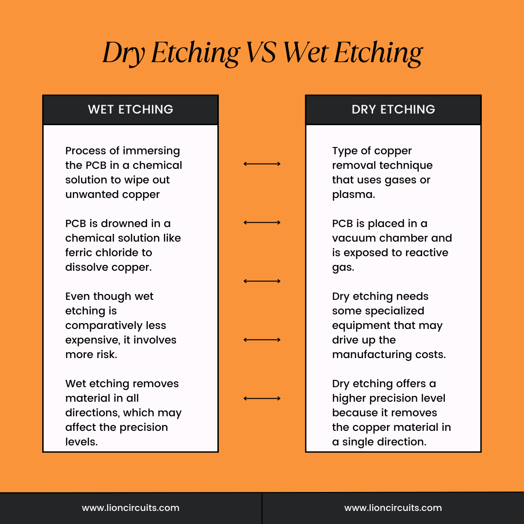
Wet etching is the process of immersing the PCB in a chemical solution to wipe out unwanted copper from the surface while dry etching is the type of copper removal technique that uses gases or plasma.
2. Procedure
In wet etching, the PCB is drowned in a chemical solution like ferric chloride. Then, the solution electively dissolves the exposed copper, leaving behind the desired circuit pattern. However, dry etching does not use any kind of chemical substance. Under dry etching, PCB is placed in a vacuum chamber and is exposed to reactive gas that leaves the circuit design without any unwanted copper
3. Cost
Dry etching is a cleaner and safer technique but needs some specialised equipment that may drive up the manufacturing costs. Even though wet etching is comparatively less expensive, it involves more risk as various dangerous chemical substances are used.
4. Precision
Dry etching offers a higher precision level because it removes the copper material in a single direction. However, wet etching removes material in all directions, which may affect the precision levels. This is more suitable for single-sided PCBs.
PCB Etching Best Practices
PCB etching is one of the most significant steps in the manufacturing of an electronic device that is to be carefully handled. Here are some best practices to follow during the PCB etching process:
- Before starting with the etching process, properly clean the PCB surface to remove any contaminants.
- Consider using high-quality copper-clad laminates for optimised results.
- Make sure that all the manual labourers wear safety gear including protective glasses, gloves, etc.
- As soon as the unwanted copper traces are removed, remove the board from the solution or vacuum to prevent over-etching.
- After the process, mix the etching solution with a base like baking soda or washing soda to neutralise the acid. This way, it will be more safe for disposal.
Final Thoughts
There are many etching methods and choosing the right one is critical for the purpose. Always keep in mind that PCB etching is not an area of guesswork. Lack of knowledge of PCB etching basics and steps is one of the main reasons for the failure of many etching processes. In case of any confusion, feel free to contact a PCB assembly and etching professional right away.
%20(1).jpg)
