.jpg)
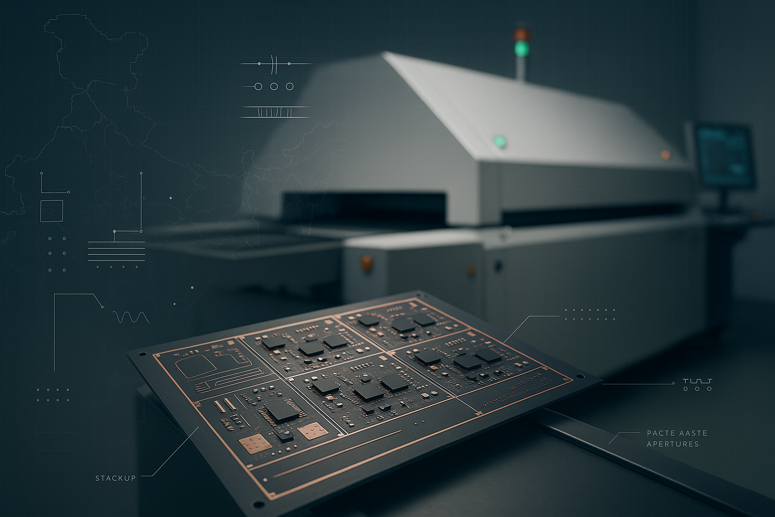
One of the most crucial steps in the manufacturing of an electric device is transforming the innovative PBC design into a functional reality. This process is called PCB assembly. It comes up with a wide range of challenges, from component selection to ensuring fidelity.
This blog will walk the readers through all the basics of the assembly process including what is PCB assembly, the steps, and the types of technologies used.
Key Highlights
- PCB assembly is the process of placing electrical components into a PCB to make it functional.
- Manufacturers must apply the solder paste, place the PCB components, perform reflow soldering process, conduct inspection, and test the board for PCB assembly process.
- 2 Main Types of Assembling Techniques are Surface Mount Technology (SMT) and Through-Hole Technology (THT). SMT is the easiest assembling method as it involves the placement of components directly to the PCB surface. But THT involves placement through holes in the PCB.
What is a PCB Assembly?
PCB assembly is the process of placing electrical components into a PCB to make it functional. It is one of the final stages in the production of an electronic device. Unfortunately, people often confuse it with the term PCB fabrication. Well, the fact is that PCB fabrication involves the activities of manufacturing a bare PCB while PCB assembly focuses on making it fully functional. In a nutshell, PCB assembly starts at the point where fabrication ends.
Some of the main components involved in PCB assembly are:
1. Solder Paste: Solder paste is a component made of tiny grains and flux that is added to the board to facilitate the attachment of components to electric devices. It is applied using a screen printing process where a roller will press it over to the board.
2. Electronic components: Various electronic components like resistors, capacitors, integrators, etc., are placed on the areas where solder paste is applied. Components will be placed either through machines or manually, depending on the complexity.
3. PCB: The PCB made of fibreglass or plastic through fabrication itself is a major component of the assembly process. PCB goes through many processes including soldering, where the solder paste melts to create connections between the components and the board.
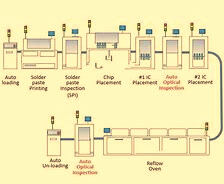
PCB Assembly Steps
The PCB assembly process involves several critical steps to ensure sufficient quality standards for the final product. Here is a detailed breakdown of the steps involved in the project:
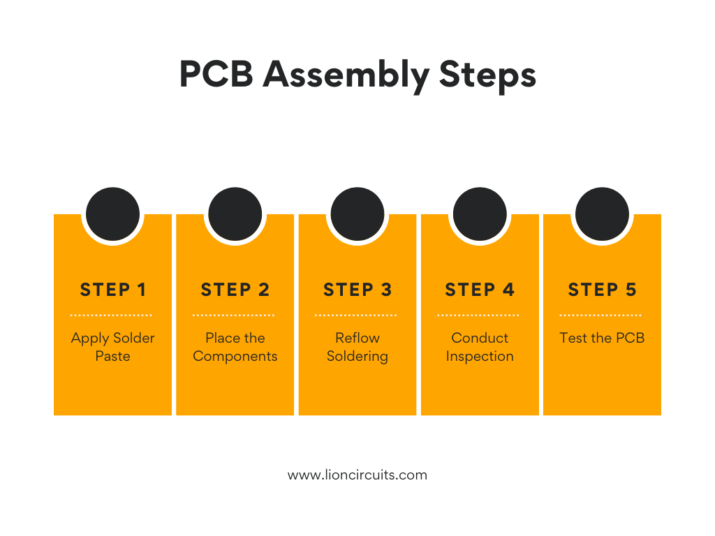
1. Apply Solder Paste
As mentioned earlier, solder paste is a mix of powdered metals like tin (96.5%), silver (3%), and copper (0.5%). First of all, this solder paste is applied to the board using a process called PCB stencil printing. A stencil, made up of stainless steel, is placed over the PCB with apertures that match the PCB pads where solder paste is needed.
The solder paste is bonded to a surface by mixing with a flux. As per professional standards, an applicator is then used to ensure that the paste is applied uniformly at the right spots in precise amounts. After application, companies usually inspect it through Solder Paste Inspection (SPI) machines.
2. Place the components
Once the application of solder paste is finished, the next step is to place surface-mount devices (SMDs) on the PCB. This could be done through two methods. Firstly, companies can set labourers to place the devices manually with a pair of tweezers.
However, this method usually results in errors in placement. That's why companies are nowadays switching to pick and place robotic machines that collect the PCB with a vacuum grip. It moves the PCB to the pick and place station and applies it to the top of the solder paste in the preset locations.
3. Reflow Soldering
Reflow is the process through which the solder paste solidifies to fix the components in the PCB. In this process, the PCB is moved to a conveyor belt that moves through a reflow oven. The PCB is subjected to heating of about 250 degrees Celsius to melt the solder paste.
After the melting process, the PCB passes through a series of ovens with cooler heaters to lower the temperature. This process solidifies the solder paste to connect the surface-mount devices to the PCB.
4. Inspection
Sometimes, errors may occur after the process of reflow soldering. Some of the common errors are:
- Non-wetting or poor wetting of reflow solder joints.
- Poor quality solder paste with high metal content.
- Poor coplanarity of components.
- Irregular placement of the lines.
It is crucial to detect such errors and rectify them earlier itself. Since inspection has a significant importance, companies usually allocate it to humans rather than relying on machines. However, when the number of boards increases, manual inspections seem to be impractical.
That's where an Automatic Optical Inspection (AOI) machine comes in. It uses cameras at different angles to catch low-quality solder. Apart from this, some companies use X-ray inspection, too, to inspect through the layers and detect any unfixed problems.
5. Test the PCB
After completion of all these steps, a functional test is conducted to check out how well the PCB operates. For this, testers usually create a plan that outlines the test objectives and acceptance criteria. Then, specific inputs are applied to the PCB to verify that the outputs match the expected results. In case a failure occurs, diagnostic testing is conducted to find the root cause of the failure.
Types of PCB Assembly Technologies
There are several types of PCB assembly technologies. However, here is a quick overview of the 2 main assembly technologies:
1. Surface Mount Technology
Surface Mount Technology (SMT) is the easiest assembling method as compared to other technologies. It involves placing electronic components directly onto the surface of a printed circuit board (PCB) using solder paste. Normally, sectors like telecommunications, consumer electronics, etc., use this technology.
Advantages
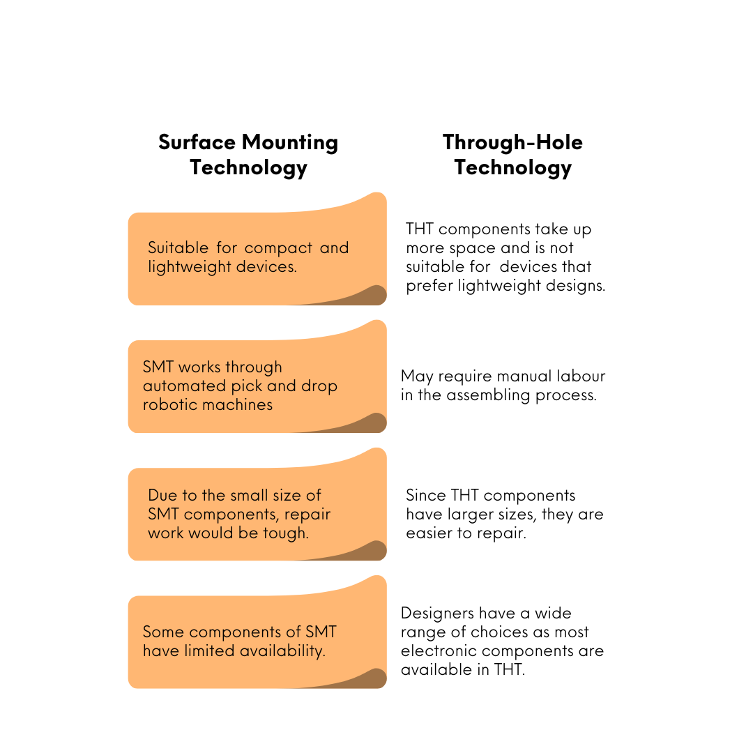
- SMT is known to utilise the area efficiently, making it a better option for devices that feature compact designs.
- SMT components shorten signal paths and improve signal integrity which results in the better performance of the device.
- SMT is mainly done through automated robotic machines. As a result, the chances of errors are reduced.
- Since SMT uses automated machines, the cost of manual labour is reduced, making it a cost-effective option.
Disadvantages
- Due to the small size of SMT components, repair work would be tough.
- Several specialised machineries are required for SMT which may skyrocket the manufacturing costs.
- Sometimes SMT components become prone to mechanical stress, which affects the overall performance of the device.
- Chances of damage for the SMT components are high during thermal cycles.
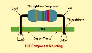
2. Through-Hole Technology
As the name suggests, Through-hole Technology (THT) is the process of inserting components through holes in the PCB and soldering them on the opposite side. It is also known as through-hole assembly or through-hole mounting.
Advantages
- THT reduces the risk of damage by strengthening the bond between the components.
- Since THT components have larger sizes, they are easier to repair.
- Designers have a wide range of choices as most electronic components are available in THT.
- THT is suitable for devices that need significant power dissipation as it can withstand higher power levels.
Disadvantages
- THT components take up more space through leads and holes. Therefore, it is not suitable for devices that prefer lightweight design.
- THT may require manual labourers in the assembly which may shoot up the manufacturing cost.
- Since automation is difficult in THT, high-scale production is challenging.
- Large through-hole components can be difficult to handle and assemble.
Sometimes, companies use a mixed technology combining both SMT and THT. This approach is mainly used when a design requires both high-density surface mount components and heavier components that need through-hole mounting
Surface-Mounting Technology VS Through-Hole Technology
Final Thoughts
Ignorance of the basics of PCB assembly is one of the main reasons for the manufacturing defects of the boards. As per stats, modern technologies like ENIG PCB in manufacturing will drive up the Compound Annual Growth Rate (CAGR) of the market by 10.72 %. Therefore, always get updated and experiment with the latest technologies to stay ahead of the curve.