
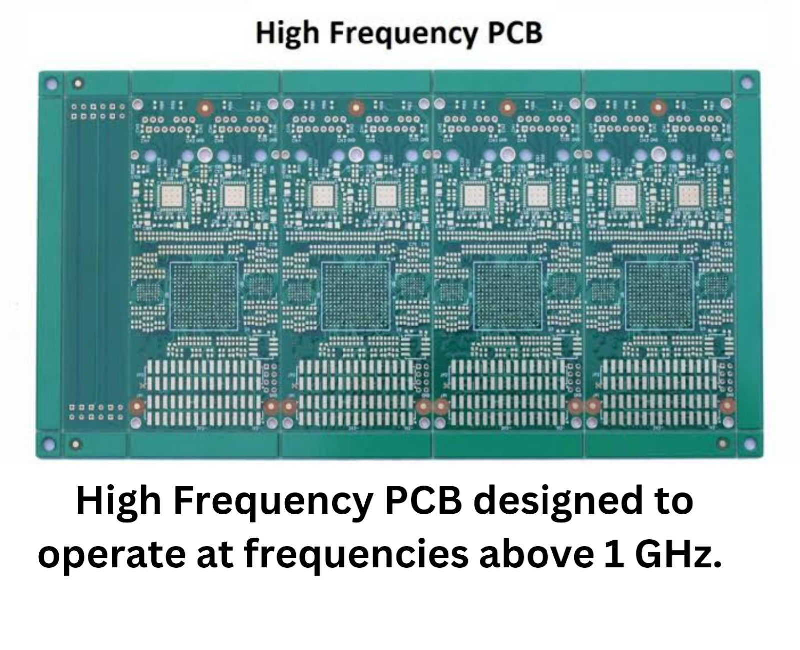
High Frequency Printed Circuit Boards, or HF PCBs, are some of the essential components of modern electronics due to their high frequencies. These specific PCBs are made to work with frequencies from 500 MHz to over 2 GHz, making them very important in many high-tech fields. In telecommunications, HF PCBs make sure that devices like smartphones, routers, and satellite transmission systems work without any problems. Apart from that, HF PCBs are very important in the medical field for imaging devices, testing tools, and systems that keep an eye on patients.
This article aims to give the audience a better understanding of high frequency printed circuit boards. It will include their special features, different materials, design challenges, and production needs.
Key Highlights
- High-Frequency PCBs are those boards that are specially designed to handle frequencies in the higher range, usually above 1 GHz.
- HF PCBs are made up of PTFE, rogers, and other specialised substrates.
- HF PCBs are known for its unique properties like low dielectric loss, efficient thermal management, impedance control, and maintenance of signal integrity at high frequencies.
- Manufacturers must ensure high precision manufacturing, clean room environment, conduct quality checks, and use proper equipment to manufacture HF PCBs efficiently.
- Some of the main challenges of HF PCB manufacturing are high costs, increased complexity, signal issues, and the need for effective thermal control.
- HF PCBs are used in many industries like telecommunications, aerospace, defence, medical, automotive, etc.
What is High Frequency PCB?
HF PCBs are those boards that are specially designed to handle frequencies in the higher range, usually above 1 GHz. This makes them necessary for sending signals quickly. These PCBs are designed to handle the fast transmission of electrical signals, making sure that there is little signal loss and that the integrity of the signals stays the same at high frequencies.
HF PCBs use materials with better electrical properties and stability to get the results they need. Common materials include:
- Teflon PCBs: are a good insulator. That’s why Teflon materials are often used for high-frequency printed circuit boards. It does not lose signals easily, and this works well with high frequencies.
- Rogers Materials: These are the best suited high-frequency laminates. They can handle heat very well and lose very little electrical signal. It makes them perfect for tough uses.
- Other Specialised Substrates: To improve performance, materials like ceramics and other advanced compounds are also used, especially in situations where very high frequencies are needed. The PCB assembly process for HF PCBs requires special care and precision to ensure optimal performance at high frequencies.
HF PCBs work in frequencies between 500 MHz and more than 2 GHz. This broad range is very important for uses that need to send data quickly and reliably, like in telephones, aerospace, and advanced medical devices. For these areas, HF PCBs are essential because they allow high-speed signal transmission with little to no loss.
Comparison with Standard PCBs
Performance:
When it comes to handling high-frequency signals, HF PCBs work better than normal PCBs. Standard PCBs are usually used for uses with lower frequencies because they can't keep signals pure at higher frequencies.
Material Requirements:
Standard PCBs usually use FR4 material, but HF PCBs need special substrates like PTFE and Rogers materials to work well with high frequencies.
Design Complexity:
Because of the need for exact impedance control, low signal loss, and good thermal management, making HF PCBs is more difficult. Standard PCBs don't need to be designed with such strict care.
High frequency PCBs are essential for current electronics that need to send data at very high speeds. They are different from regular PCBs in terms of performance and application span because they are made of special materials and have complex designs that let them meet the needs of high-tech industries.
Characteristics of High Frequency PCB
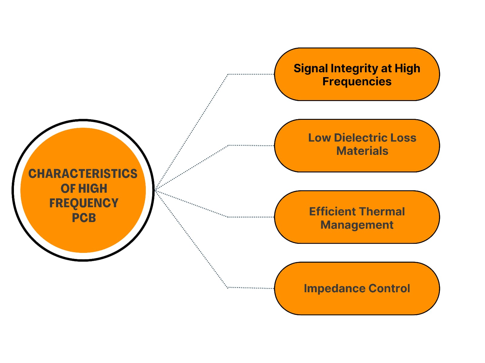
High frequency printed circuit boards have certain unique characteristics. High frequencies are maintained by them in signal integrity. That is the reason for their significance for sophisticated electronic applications.
1) Signal Integrity at High Frequencies
Maintaining the intensity of signals at high frequencies is crucial to send data precisely and reliably. Signal distortion and loss are minimised by the finest materials and meticulous design. In fact, reduction of noise and electromagnetic interference (EMI) is the primary objective of high-frequency PCB. It can obscure messages. Signals are designed to move slowly or lose little strength, maintaining the accuracy of the information being transmitted. The selection and placement of PCB components are critical factors in maintaining signal integrity in HF PCBs.
2) Low Dielectric Loss Materials
The use of low dielectric loss materials, such as Rogers and PTFE (Teflon PCB), is crucial in HF PCBs. They conduct electricity really well through these materials. Low dissipation factor and low dielectric constant are their striking features. Both signal loss is reduced and device performance is improved due to these features. Smooth speed and clarity of high-frequency transmissions are guaranteed by low dielectric loss. It guarantees accurate and timely data transmission.
3) Efficient Thermal Management
Electronics can be damaged or destroyed by overheating, hence having a good heat escape is crucial. Higher power levels mean that HF PCBs must be heat-resistant. Thermal vias, heat sinks and better substrate materials enable HF PCBs to effectively manage heat. This guarantees long-lasting performance and good functionality of the PCB in demanding circumstances. PCB gold fingers are often used in HF PCBs to ensure reliable connections and minimise signal loss at board edges.
4) Impedance Control
HF PCB design requires careful consideration of impedance to ensure accurate and dependable signals. Precisely regulating impedance will prevent signal echoes and distortions that can result from impedance mismatch. This is made feasible by careful selection of materials, trace width, and spacing together with sophisticated modelling and computer tools. Correct management of the impedance allows for the transmission of high-frequency data with little loss and distortion. Signal integrity, heat management, and exact impedance control are all greatly impacted by the characteristics of high frequency PCBs.
High Frequency PCB Design Considerations
Engineers consider a lot when creating these multilayer PCBs. To ensure the board functions well, they meticulously finalise a lot of aspects. Here are some factors to consider during the manufacturing process:
1) Material Selection
Selection of the appropriate materials is crucial in HF PCB design. Low-loss substrates like Rogers materials and PTFE (Teflon) are preferred since they conduct electricity so well. Signal loss is kept to a minimum and high-frequency communications are efficiently transmitted by these materials. The low dissipation factor and dielectric constant of these surfaces prevent performance loss and preserve signals.
2) Trace Layout and Routing
Use of the correct trace structure and route is crucial to reduce signal loss and crosstalk. High-frequency signals are particularly prone to interfere, hence trace lines must be meticulously designed. Wider lines and ample space between them reduce the likelihood of impedance mismatches and signal reflections. A smooth form and avoiding sudden curves when routing traces also help maintain the impedance constant and reduce the likelihood of signal deterioration. In some applications, flex PCB technology is employed to allow for flexible routing solutions in compact high-frequency designs.
3) Via Design and Placement
Signal integrity can be greatly impacted by the vias that connect various PCB layers. Through poorly designed vias, signal echoes and variations in impedance can result. Get the best performance from vias by reducing the number of vias in high-frequency signal channels and improving return current paths with via stitching. Signals can also be preserved and loss reduced by making sure vias are spaced correctly and have the correct coating.
4) Simulation and Testing
At the design stage, HF PCBs must be thoroughly simulated and tested to ensure that they function as intended. The way the electrical characteristics of PCBs vary over time can be modelled using sophisticated modelling techniques. This enables designers to foresee and resolve issues such impedance mismatches, crosstalk, and signal loss. To ensure that the PCB operates as intended in real life, it must undergo numerous tests, including temperature analysis and signal integrity testing, after the design is finished.
In order to create high frequency PCBs, one must apply design optimization, meticulous material selection, precise trace routing and layout, extensive modelling and testing. These factors provide great performance and dependability that are required for sophisticated electronic applications from HF PCBs. The design of PCB pad structures is crucial in HF PCBs to maintain consistent impedance and minimise signal reflections.
Manufacturing Requirements for High Frequency PCB
To meet the strict standards for high-frequency applications, making High Frequency PCBs (HF PCBs) requires a lot of precision and control. These are the important things and steps that need to be taken:
1) High Precision Manufacturing
To achieve the highest performance levels, HF PCBs must be manufactured using extremely exacting techniques. Selecting premium materials, such as low-loss plates, is the first step toward this degree of precision, which continues throughout the manufacturing process.
Correct PCB etching, drilling, and plating are essential to maintaining the high-frequency data. Impedance mismatches, signal loss, and general PCB performance can all result from any defects or modifications. The use of a PCB stencil is often necessary for precise application of solder paste in HF PCB assembly.
2) Cleanroom Environment
Keeping a cleanroom environment is crucial when creating HF PCBs. Dust, moisture, and oils are among the pollutants that can degrade PCB performance by introducing contaminants that compromise signal integrity.
Weather, humidity, and dust and filth levels are all strictly regulated in cleanrooms. As such, it prevents things from becoming filthy. Manufacturers can use cleanroom technology to ensure that no pollutants enter the production process. It guarantees an outstanding performance from the PCBs.
3) Quality Control Measures
To make sure that HF PCBs are reliable, strong quality control methods must be used. Important steps for quality control are:
1. Impedance Testing:
Conduct regular tests to ensure that the PCB satisfies the impedance standards. Reducing echoes and maintaining pure signals need controlling impedance.
2. Thermal Analysis:
Higher power densities of HF PCBs make temperature management crucial. Thermal analysis must be done to make sure that the PCB can effectively remove heat, preventing it from getting too hot and extending its life by pointing up potential problems.
3. Electrical Testing:
Full electrical testing makes sure that all parts and links work properly. Thus, the PCB will meet the required electrical standards.
4. Visual Inspection:
Automated optical inspection systems find any physical flaws present in the PCB, such as glueing problems, misalignments, or surface flaws.
4) Advanced Equipment and Technologies
To get the precision and quality that are needed, HF PCBs are made with the help of cutting edge technologies and tools.
1. Laser Direct Imaging (LDI):
This technology uses laser beams to precisely pattern the PCB. It makes sure that the trace plan is very accurate.
2. Automated Optical Inspection (AOI):
AOI systems check PCBs for flaws. They verify whether the board meets design requirements using cameras and software tools.
3. X-Ray Inspection Systems:
These systems check the inside of PCBs to inspect multilayer connections and solder joints. It makes sure there aren't any flaws that cannot be seen.
4. High-Precision Drilling Machines:
These machines can drill very small holes and vias. They perform this task with great accuracy. It is necessary to keep signals on HF PCBs intact.
High-frequency printed circuit board manufacture requires great accuracy. Furthermore required are a spotless room and stringent quality control procedures. By following these regulations, high-performance applications can be assured that HF PCBs satisfy the stringent requirements. They maintain their capabilities to transmit high-frequency communications and dependability as well.
Challenges in High Frequency PCB Design
Some serious concerns need to be addressed when designing high Frequency PCBs. To make reliable and high-performing HF PCBs, these problems must be solved with a mix of advanced materials, careful design methods, and advanced production technologies. Check out some of such pressing concerns faced in the designing process:
1) Signal Integrity Issues
Signal Loss: As signals move through the PCB, high-frequency pulses often lose some of their power. This signal loss can make the gadget work less well and have a shorter range.
Designers use low-loss materials like PTFE (Teflon) and Rogers materials. It will help to keep signal loss to a minimum. These materials have lower dielectric constants and dissipation factors. Thus, they perform low signal loss.
Crosstalk:
Crosstalk happens when signals from nearby traces mess with each other. It makes noise and possibly messes up data. To reduce crosstalk, designers carefully lay out the lines.
During that, they make sure that there is enough space between those lines. Also, they use ground planes to protect the signals. Differential signalling can also help cut down on crosstalk. It makes the messages more equal and gets rid of noise.
Electromagnetic Interference (EMI):
EMI is a big problem in HF PCB design because high-frequency waves can send out and mess up other systems or components.
Some effective ways to reduce EMI are to use the right grounding, shielding methods, and design the PCB layout to cut down on loop areas and radiation.
2) Higher Costs of Specialised Materials
For HF PCBs, you need special materials like PTFE and Rogers materials, which cost more than regular FR4 substrates. These materials have better electrical properties that are needed for high-frequency performance, but they make the total cost of production higher. Apart from such material costs, the entire process requires highly trained experts which may shoot up the entire budget further.
3) Increased Complexity in Manufacturing Processes
Due to the need for exact control over many parameters, making HF PCBs is more difficult than making regular PCBs. For high-frequency designs, trace sizes, spacing, and layer alignment must be very precise.
In order to meet these needs, advanced industrial methods like Laser Direct Imaging (LDI) and high-precision drilling are needed. Because these processes are so complicated, they need specialised knowledge and tools, which makes output even harder.
4) Effective Thermal Management
For HF PCBs to last a long time and not get too hot, they need to have good thermal control. A lot of the time, high-frequency circuits use more power, which makes a lot of heat.
To handle this heat, manufacturers need to use effective ways to get rid of it, like thermal vias, heat sinks, and improved thermal substrates. During the design process, thermal analysis helps find possible hotspots. It improves the layout of the PCB. Thus, heat is spread more evenly.
Applications of High Frequency PCBs
High frequency printed circuit boards, or HF PCBs, are used in many fields because they can handle high-speed data with little loss. That’s why they are essential in many high-performance situations.
1. Telecommunications
HF PCBs are very important in telecommunications for sending data quickly and talking wirelessly. These PCBs are common for devices like smartphones, routers, and satellite communication systems since they send and receive data quickly and reliably.
HF PCBs keep signals intact at high frequencies. It makes sure that data is sent quickly and correctly, which is essential for modern communication networks to work smoothly.
They are also very important for the infrastructure of 5G networks. Since these networks use high-frequency signals, HF PCBs come in handy to send data more quickly and with less delay.
2. Aerospace and Defense
In aerospace and defence, accuracy and dependability are very important. That’s why HF PCBs play a big part. HF PCBs are used to process high-frequency signals in radar systems. This component lets them accurately find and track things.
Moreover, HF PCBs are used in communication systems in planes and military gear. These devices are required to perform clerical tasks. That’s why these boards send important data safely and without interruption.
HF PCBs also work well in harsh environments. This is why they can be used in satellites, unmanned aerial vehicles (UAVs), and many military technologies.
3. Medical Devices
Specially in imaging and diagnostic instruments, the sophisticated properties of HF PCBs are highly beneficial in the medical industry. High-frequency data required to produce finely detailed images of the human body in devices such as MRIs, CT scanners, and ultrasounds is handled by HF PCBs.
Better results for patients and more precise diagnoses are the outcomes of these PCBs' efficient and fast signal processing. Additionally using HF PCBs are wearable health monitoring and moveable medical equipment that require fast and dependable signal transmission.
4. Automotive Industry
The automotive industry heavily depends on HF PCBs to create infotainment and advanced driver assistance systems (ADAS). High-frequency signals must be processed by ADAS systems like radar and lidar in order to do things like adaptive cruise control, lane keeping assistance, and collision avoidance.
Together with increasing vehicle safety, these systems also make driving more fun. High-definition displays, Bluetooth connectivity, and GPS tracking—all of which require fast and dependable data transmission—are further functions supported by HF PCBs in automobile entertainment systems.
Conclusion
High frequency printed circuit boards are essential to transmit data fast and safely in many industries, including telecommunications, aviation, defence, medical equipment, and automotive systems. Actually, there are several advantages of HF PCBs, including reduced loss in handling high-frequency signals, improved temperature control, and improved signal integrity.
These benefits make high-performance, reliable electrical applications where HF PCBs are essential. Innovation of even more sophisticated technology might result from an understanding of their complexities and novel concepts. To fully benefit from its applications, readers should also concentrate on learning these fundamental circuit boards inside and out.
%20(1).jpg)
