.jpg)
ENIG, abbreviated as electroless nickel immersion gold, is a surface finish on a circuit board to safeguard copper pads. It is one of the most significant PCB components for ensuring the performance of electronic devices in crucial industries like defence, medical, aerospace, etc.
As the name suggests, ENIG is made up of two layers- gold and nickel. First of all, nickel is plated on top of copper pads through an electroless chemical reaction to protect them from oxidation. Then, a thin layer of gold is plated on the surface to give more shelf-life to the nickel layer.
This blog will cover all aspects of ENIG PCB, including the manufacturing steps, advantages, disadvantages, and applications.
Key Highlights
- The ENIG plating process involves application of a nickel layer and gold layer for protection.
- The main advantages of ENIG finishings are compatibility, uniform thickness, and longer shelf-life while the disadvantages are higher cost, low thermal shock resistance, and chances of black pad syndrome.
- ENIG PCBs are specifically used in industries where devices are prone to harsh environments like defence, aerodynamics, etc,
- ENIG shelf life depends on various factors like handling, coating, storage conditions, and the overall quality of manufacturing.
- ENEPIG is the top alternative to ENIG due to its improved corrosion resistance and high-temperature soldering ability but has more cost and complexity.
- The manufacturing of ENIG PCBs are expected to increase in the future due to rise in demands from various sectors.
What is ENIG PCB?
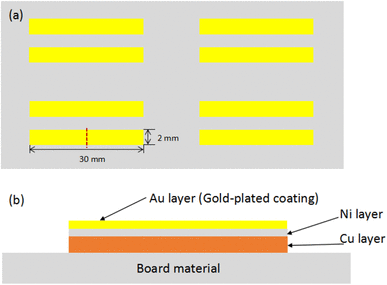
ENIG is a multi-layered surface finish technique that is usually applied on PCB surfaces to protect the copper pads from corrosion. It involves plating of nickel followed by the application of a thin gold layer on top of it. The nickel layer protects the pads from corrosion while the gold layer, in turn, safeguards the nickel itself during storage. The entire process is done to improve the shelf life of the PCB.
ENIG Plating Process
Copper pads have to go through a chain of steps to deposit the two metallic layers. Check out them:
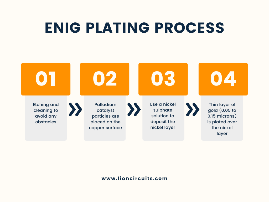
- Copper pads are subjected to etching and cleaning to avoid any obstacles to the plating process. PCB etching is done through a chemical solution like sulfuric acid. Copper pads are dipped into the solutions to eliminate residual oxides.
- Palladium catalyst particles are placed on the copper surface using a dilute solution to start the electroless chemical reaction for depositing nickel.
- Use a nickel sulphate solution along with reducing agents to deposit the nickel layer (0.05 to 0.2 microns) onto the top of the PCB pads.
- A thin layer of gold (0.05 to 0.15 microns) is plated over the nickel layer as protection through a gold salt solution like potassium gold cyanide.
Advantages of ENIG
ENIG finishing is nowadays arising as a common practice in the manufacturing of electronic devices due to many reasons. Here are some of them:
- Compatibility: One of the main advantages of ENIG PCBs is that they are optimised for both lead and lead-free solders. Therefore, many electronic devices, ranging from day-to-day consumer electronics to heavy industries like defence, can try out ENIG finishing.
- Suitable for wire bonding and CSPs: ENIG finishes result in a highly conductive circuit board surface that is perfect for wire bonding. Moreover, the electroless deposition process leaves behind a flat circuit surface which is important for fine-pitch components like chip-scale packages (CSPs).
- Long-Lasting: ENIG layering is done with the primary aim of extending the lifetime of PCB gold fingers and pad surfaces. The nickel layer in ENIG protects copper from oxidation and the gold layer saves nickel from damage during shipping. As a result, ENIG PCBs can withstand more mechanical stress and increase the lifetime of devices.
- Same Level of Thickness: When it comes to the Surface Mount Technology (SMT) assembling technique, the thickness level has significant importance. Luckily, ENIG ensures uniform layer thickness to avoid any problems during the PCB assembly process.
Disadvantages of ENIG
Even though ENIG finishing comes up with many significant benefits, there are many pressing concerns to discuss. Here are some of them:
- Higher Cost: Compared to other finishings like Hot Air Soldering Level (HASL) or Organic Solderability Preservative (OSP), ENIG is more costly as two metallic layers are to be deposited. On top of that, the chemicals required for the electroless process are expensive.
- Careful Handling: Since nickel is vulnerable to oxidation, ENIG requires keen handling by trained professionals. Any fault during manufacturing may result in severe consequences during the PCB assembly process.
- Chances of Black Pad: If any minute amount of impurities are present on the surface during the electroless deposition process, an issue called black pad may happen. As a result, solder joint reliability will be affected and eventually, the functioning of PCB will be disrupted.
- Low Thermal Shock Resistance: The chances of damage to the nickel layer is high as ENIG PCBs are more vulnerable to thermal shock.
Applications of ENIG PCB
Due to its wide range of support for various devices, ENIG finishing is used in a lot of industries. Have a look at some of the prominent industries:
- Electronics: ENIG is used in the manufacturing of many electronic components like PCB layers, Integrated Circuits (IC), connectors, etc.
- Medical: Since medical devices such as pacemakers and defibrillators require durability, ENIG finishing is often used to resist mechanical stress.
- Aerospace: A gold layer of ENIG protects from corrosion which is really helpful for aerospace components that are meant to function under harsh environments.
- Telecommunications: As mentioned earlier, since ENIG supports the SMT assembly process and wire bonding, the telecommunication industry uses it to ensure fast data transfer.
- Defence: The flat surface provided by ENIG finishing is suitable for chip-scale packages, which is crucial for defence equipment that requires high density and minimum size.
Design Considerations for ENIG PCBs
Manufacturing an ENIG PCB is not based on guesswork; it requires the expertise of professionals and carefulness. Check out some important points to be considered during the process:
- As per IPC, there are many measurement standards to be noted during manufacturing. For instance, an annular ring of 0.15 mm is suggested and the trace width is recommended to be around 0.1 mm. Similarly, the hole size must be at least 0.2 mm.
- Placement of a solder mask over bare copper (SMOBC) can protect it from environmental damage like moisture.
- Usage of no-clean fluxes is recommended as they leave no residue after the soldering process.
- Even though ENIG finishing is done to improve the reliability of device components, mixing it with other elements that do not have the same level of corrosion resistance may pull down the performance of the entire device.
- Clean the surface thoroughly as any contaminants can disrupt the layers and affect the performance of the device.
Soldering and Shelf Life of ENIG
ENIG helps to create a flat finishing on PCB surfaces which is helpful for ensuring reliable solder joint formation. However, its shelf life depends on various factors:
1. Handling
If the employees are not equipped with glows, the risk of contact between contaminants and the PCB surface will be much higher. As a result, the ENIG layers get worn out leaving the PCB prone to corrosion.
2.Coating
The placement of a conformal coating above ENIG acts as an extra protection layer against corrosion and can extend the lifetime of electronic devices.
3. Storage Conditions
Exposure to environmental conditions like moisture can result in a lower shelf life for ENIG PCB as it can penetrate through the inner layers.
4.Quality of Process
The quality of the ENIG finishing process has a significant stake over its lifetime. Even minute variations in the thickness or composition can have a significant impact over the lifetime.
Just like these factors, successful soldering is crucial for PCB reliability. Check out some tips for that:
- Consider using lead-free alloys like SAC (Sn-Ag-Cu), SN100C (Sn-Cu-Ni), etc., that work well with the ENIG for better reliability.
- Select rosin-based or no-cleaning fluxes as they prevent oxidation during the process.
- Maintain general temperature guidelines to avoid any kind of damage. In case you are using lead-free solder, the temperature must be around 240-260°C while for tin-free solder, the temperature could be lowered to approximately 220-240°C.
- Make sure that the PCB stencil thickness is acceptable as per expert guidelines.
ENIG VS ENEPIG
Like ENIG, yet another widely accepted surface finishing technique is ENEPIG (Electroless Nickel Electroless Palladium Immersion Gold). Even though the names sound similar, there are many wide differences to consider. Here are some of them:
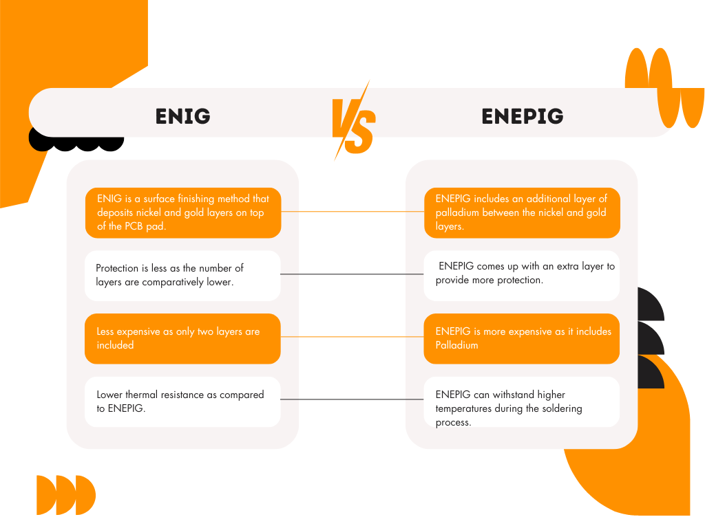
1. Process
ENIG is a surface finishing method that deposits a nickel layer on top of the PCB pad followed by a coating of gold. However, ENEPIG includes an additional layer of palladium between the nickel and gold layers to improve protection.
2. Corrosion Resistance
Since ENEPIG comes up with an extra layer, it provides more corrosion resistance as compared to ENIG.
3. Cost
ENEPIG is more expensive as it includes Palladium which adds up to the overall cost.
4. Complexity
ENIG layering consists of two main steps: nickel placement and gold deposition. But ENEPIG has an extra step of palladium deposition which adds up to the complexity of the process.
5. Soldering Ability
ENEPIG can withstand higher temperatures during the soldering process, making it suitable for some high-temperature applications.
The choice of whether ENIG or ENEPIG for your PCB depends upon your requirements. ENIG is specifically used in PCBs that require SMT assembly due to its flatness. It works well if you are working on a tight budget. But if you are working on a device that requires high connectivity like telecommunications, ENEPIG is a better choice as its palladium layer improves wire bonding.
ENIG Quality Control and Reliability
Even though ENIG finishing is widely considered an effective technique to improve the PCB shelf life, they are prone to many risks. For instance, the nickel layer may corrode much before copper and may affect solder joint reliability. This is called Galvanic corrosion. Similarly, brittle fibres of metal, called whiskers, may grow on PCB pads when the surface comes into contact with contaminants.
Proper testing and inspection must be made prior to the launch to ensure the quality of ENIG PCBs. Here are some important points to consider while verifying the quality:
- As per IPC standards (4552), the thickness of nickel layers must be within 3-6μm and gold layers within 0.05-0.2 μm.
- Make sure that the surface is rough enough to support the wetting and spreading of the solder.
- There should not be porosity on the surface which may drain away the ability of the PCB to resist corrosion and may lead to consequences like black pad formation.
- Ensure that the PCB surface is well-cleaned from dirt and contaminants.
Emerging Trends and Future of ENIG
The ENIG PCB market size is projected to cruise forward with a CAGR of 15.7% from 2024-2031. This steady growth is driven by rising demand for corrosion-resistant materials in sectors where equipment is subjected to harsh environments like defence and aerodynamics. Moreover, the demand for multilayer pcb is also contributing to the growing market of ENIG finishings.
Apart from this, the growing need for compactness and high circuit density in electronic devices is leading to the experimentation of new ENIG PCBs. For instance, many manufacturers try out low-phosphorus nickel to improve corrosion resistance.
Yet another positive trend in the sector is the shift to lead-free ENIG PCB. It helps manufacturers to comply with ROHS (Restriction of Hazardous Substances) regulations. Similarly, advancements in the field of material science will reflect in the ENIG PCB market by solving pressing concerns like black pad syndrome.
Conclusion
Considering this trend, it goes without saying that the future of the ENIG PCB market looks brighter than ever before. Almost all manufacturers are expanding their production with more advanced materials and equipment. Keeping up with these emerging trends is not just innovation but necessary to survive in a competitive market.
%20(1).jpg)
