
An annular ring refers to the conductive ring that surrounds a drilled hole and connects the board's layers. The PCB's durability and functionality depend heavily on the size and quality of the annular ring. It helps to avoid signal loss and improper connections.
Annular rings connect the different layers of the PCB, allowing electrical signals to flow uninterrupted. Here are some of the most common issues to be addressed during annular ring manufacturing:
- Inadequate ring size can cause weak connections and even board failure.
- The integrity of the board may be further risked by off-centre rings caused by misalignment during drilling.
- Ring damage from poor plating might increase the PCB's susceptibility to corrosion and wear over time.
Read on to understand everything about annular rings before its manufacturing in order to avoid such risks.
Key Highlights
- An annular ring refers to the conductive ring that surrounds a drilled hole and connects the board's layers.
- The size of the annual ring could be found by dividing the width with two.
- Correct annual ring size is required to ensure that the PCB layers have good electric connections, enough mechanical strength, and signal integrity.
- Teardrop pads are specialised forms in PCB design to improve the board's electrical and mechanical performance.
- Annular rings are made up of conductive copper layer, solder mask layer, and substrate layer through etching and plating processes.
- You must measure the hole size, determine the pad diameter, calculate annular width, and follow specific design requirements to get a correct annular ring size.
Understanding Annular Rings
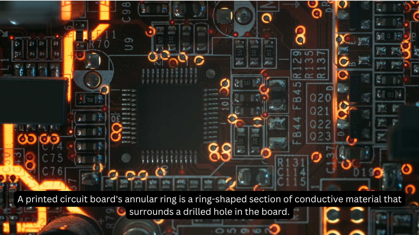
A printed circuit board's annular ring is a ring-shaped section of conductive material that surrounds a drilled hole in the board. This ring is an indispensable part for the various layers of the PCB and the components installed on it to electrically link reliably. It provides that conducting paths from different layers are connected smoothly when a hole is drilled through the board.
To avoid problems like poor connections and signal loss, designers must carefully evaluate the size and positioning of annular rings. A strong mechanical and electrical link is provided by a well-designed annular ring, providing proper PCB operation.
It is made up of multiple fundamental components. Have a brief look at them:
- The conductive substance first creates the actual ring.
- Usually, copper is used for this because it has good electrical conductivity.
- The ring encircles a drilled hole known as a through or pad that supports connections between the PCB's layers.
- A conductive material is placed over the hole to provide a continuous electrical channel.
- The solder mask is an additional component that covers the PCB surface except for the annular ring area.
- In addition to avoiding short circuits, this mask shields the conductive traces. The pad size, or the ring's overall diameter, and the hole size, or the diameter of the drilled hole, are additional dimensions of the annular ring.
The holes drilled into a PCB are usually surrounded by annular rings. These holes, sometimes referred to as PCB pads or vias, provide electrical connections between the board's multiple layers. The locations of electronic components, such as integrated circuits, resistors, and capacitors, are marked with annular rings. They provide a constant electrical channel between the surface and internal layers by being present at every layer of the printed circuit board.Around the mounting holes that hold the PCB in place within a device, annular rings are also present. When signals need to go through multiple layers on multi-layered boards, these rings are important for maintaining dependable connections. Annular rings give the drilled holes the required contact area for soldering components and maintaining electrical integrity by encircling them with conductive material.
How To Calculate the Size of Annular Rings
Use these procedures to determine the size of an annular ring on a PCB:
- Measure the Pad Diameter: Determine the pad's overall diameter, which is the circumference of the conductive substance that surrounds the hole.
- Measure the Hole Diameter: Mark the diameter of the drilled hole that will hold the component lead or permit electrical connections. This hole is also referred to as the via or pad hole.
- Calculate Annular Ring Width: Subtract the hole diameter from the pad diameter to get the annular ring width. It provides you with the total width of the annular ring surrounding the hole on both sides.
- Divide by Two: The size of the annular ring on one side of the hole can be calculated by dividing the result from step 3 by two.
Annular ring size = (Pad Diameter - Drill Diameter ) / 2
Suppose the pad diameter is 2.0 mm and the hole diameter is 1.0 mm. Then, the annular ring width would be (2.0 mm - 1.0 mm) / 2 = 0.5 mm.
Consistency in annular ring sizing calculations because it has an impact on the PCB's mechanical strength and dependency of electrical connections. For example, a device may malfunction if the annular ring is too small because it may not provide enough contact area, resulting in sporadic or weak connections. Moreover, the component leads and vias are supported by an adequate ring size, which keeps them from breaking or detaching as a result of thermal expansion.
Importance of Annular Ring Size
In PCB design, the size of the annular ring is important for a number of reasons.
- It ensures that the layers and components of the PCB have sturdy electrical connections.
- Device problems may arise from weak or sporadic connections caused by an annular ring that is too tiny.
- The PCBs mechanical strength is impacted by the size of the annular ring. If the rings are properly sized, it offers sturdy assistance for component leads and vias.
- This ring size accuracy also contributes to the preservation of signal integrity in the complex multi-layer PCBs, necessary for the board's overall performance.
Incorrect annular ring sizing can result in a number of serious problems like:
- Poor ring size may create flimsy connections that may break due to physical stress. As a result, the durability of the PCB may get affected
- Serious errors might reflect in the manufacturing process.
- Small rings may degrade the quality of the board as a whole due to solder bridging.
- Off-centre rings that deteriorate connections can be caused by misaligned holes, which can worsen these issues.
Annular Rings and Vias
Electrical connections are made between the various layers of a printed circuit board through small plated components called vias. Manufacturers must allow power signals to move between layers for a proper PCB design,
Different varieties of vias exist, such as blind or buried vias that connect only specific layers and through-hole vias that pass through the entire board. Depending on the design and complexity of the board, each sort of via has a unique purpose.
Vias are necessary to create multilayer PCBs because they help control the board's layout and make electrical signal routing easier. A circular ring must surround them in order to maintain the mechanical stability of the vias and guarantee dependable electrical connections. In a nutshell, both of them are essential to preserving the PCB's dependability and efficiency.
The annular ring's size directly impacts the dependability of the vias. Annular rings of the appropriate size provide an adequate contact area surrounding the via for soldering. Insufficient annular ring size may result in insufficient solder surface area, which could cause brittle or sporadic electrical connections. The PCB may malfunction or fail as a result of this. On the other hand, an annular ring that is excessively big may cause problems during production, like solder bridges or trouble keeping hole diameters uniform.
Understanding Teardrop Pads
Teardrop pads are specialised forms in PCB design to improve the board's electrical and mechanical performance. Teardrop pads are not like regular circular or rectangular pads; instead, they are tapered, like a teardrop. This design facilitates the smooth transition between a pad and a trace or via.
Teardrop padding is primarily used to strengthen connections and lower the possibility of stress fractures. The gentle transition from the pad to the trace reduces the possibility of weak spots where solder problems or cracks could arise. When components are closely packed on high-density boards, this design is especially helpful.It also provides more dependable solder junctions by improving solder flow throughout the PCB assembly process. Designers can improve the circuit board's dependability and durability by using teardrop pads.
Teardrop pads and annular rings are closely related and complement each other to improve the durability of the board. The strength of the annular rings can be increased through addition of teardrop pads. The annular ring and pad are connected more smoothly thanks to the teardrop form, which also strengthens the bond and lowers the risk of mechanical stress or solder problems.
Benefits of using teardrop pads in conjunction with annular rings
- Because of its tapering design, the teardrop pad smoothly transitions from the pad to the trace, aiding in the more even distribution of mechanical stress.
- By reducing the possibility of cracks and weak spots, this design increases the PCB's overall durability.
- Teardrop pads strengthen the connections around vias when paired with appropriately sized annular rings.
- A more dependable electrical contact is provided by the teardrop pad's gentle taper, which also serves to reinforce the annular ring.
- It lowers the possibility of poor solder connections and subsequent failures. Teardrop pads may improve solder flow during assembly, resulting in more dependable and uniform solder junctions.
The Structure of a PCB Annular Ring
An annular ring is situated around a drilled hole that joins the various layers of the board. It is a ring-shaped patch of conductive material that surrounds the hole and serves as a vital connection between the multiple PCB layers. Check out the different layers and materials involved in creating annular rings:
1) Conductive Copper Layer :
During the manufacturing process, copper is placed onto the PCB to form the annular ring's main composition. Excellent electrical conductivity is why copper is used in PCBs; it enables efficient transfer of electrical signals across layers. Solidifying the electrical connection requires the copper layer, which surrounds the opening in a ring.
2) Solder Mask Layer :
The second layer is the Solder Mask Layer, which lies atop the Copper Layer. All of the PCB's surface is covered with this protective layer, with the exception of the spots that require soldering. Both inadvertent short circuits and copper oxidation are prevented by the solder mask. To enable solder to flow across circular rings, the solder mask is removed.
3) PCB Substrate :
The substrate, or fibreglass-reinforced epoxy, is the main PCB component that is often constructed of materials like FR4. It divides the different conducting layers and gives the PCB structural support. In order to guarantee that the electrical routes can link through the board, the annular ring is included into this substrate.
4) Plating and Etching :
An assortment of plating and etching techniques are used in the PCB manufacturing process to produce the annular rings. First, the entire board is covered in a coating of copper. After that, the board is etched to eliminate any extra copper and leave the appropriate ring shape surrounding each hole. To guarantee a conductive passage through the board, via holes are coated with copper.
Role of the Annular Ring structure in the functionality of PCBs
- The PCB's annular ring allows power and signals to flow between its many layers, providing dependable electrical connections.
- Vias and component leads are supported by a well-designed annular ring, which lowers the possibility of mechanical failure. Accurate positioning and sizing reduce the risk of problems such as pad lifting or breakage from heat expansion or physical stress.
- The quality of the annular rings influences the production process. Correct size and appropriate plating safeguard against flaws like solder bridging and insufficient solder coverage, resulting in dependable and superior PCBs.
- Long-lasting annular rings contribute to the sustained operation of PCBs. When rings are sized and maintained correctly, issues like corrosion and mechanical wear are avoided, meaning that even in extreme conditions or with heavy usage, the PCB will continue to function reliably.
How To Get a Correct Annular Ring Size
1) Measure the Hole Size:
To begin, find the dimension of the via (drilled hole) that will be utilised in your printed circuit board. The size of this hole is important since it affects the necessary annular ring width.
2) Determine the Pad Diameter:
The pad needs to be sizable enough to offer a solid surface for soldering. Ideally the pad diameter should be at least twice the diameter of the hole to provide sufficient ring width.
3) Calculate Annular Ring Width:
Subtract the hole diameter from the pad diameter to calculate the annular ring's overall width surrounding the hole. The entire annular ring width, for instance, would be 1.0 mm if the pad diameter and hole diameter were both 2.0 mm. To find the width of the annular ring on each side of the hole, divide this width in half.
4) Follow Specific Design Requirements:
Depending on component size, number of layers, and manufacturing capabilities, many PCB designs may have particular requirements for the annular ring size. To verify conformity, review the design guidelines or requirements unique to your PCB.
Industry standards and best practices:
- IPC Standards: To ensure dependable electrical connections and excellent manufacturing quality, adhere to IPC-2221 and IPC-7351 for approved annular ring widths.
- Design for Manufacturability (DFM): To avoid manufacturing problems, match annular ring sizes to your PCB manufacturer's capabilities and design specifications.
- Take Component Size into Account: Modify annular ring sizes according to via and component sizes. For dependable connections, larger rings could be required for larger components or high-density designs.
- Steer Clear of Extremely Small Rings: Make sure annular rings are the right size to account for production tolerances and avoid poor connections and soldering problems.
What Are The Minimum Annular Ring Requirements
Minimum annular ring is the minimum permissible width of the electrical ring encircling a via in PCB design. Industry standards like IPC-2221 advise minimum ring diameters to avoid poor connections and manufacturing problems. Most probably, factors like the hole size and PCB layer count have an impact on the minimum width. If these minimal standards are not met, there may be a higher chance of soldering errors, which may lead to decreased mechanical strength.
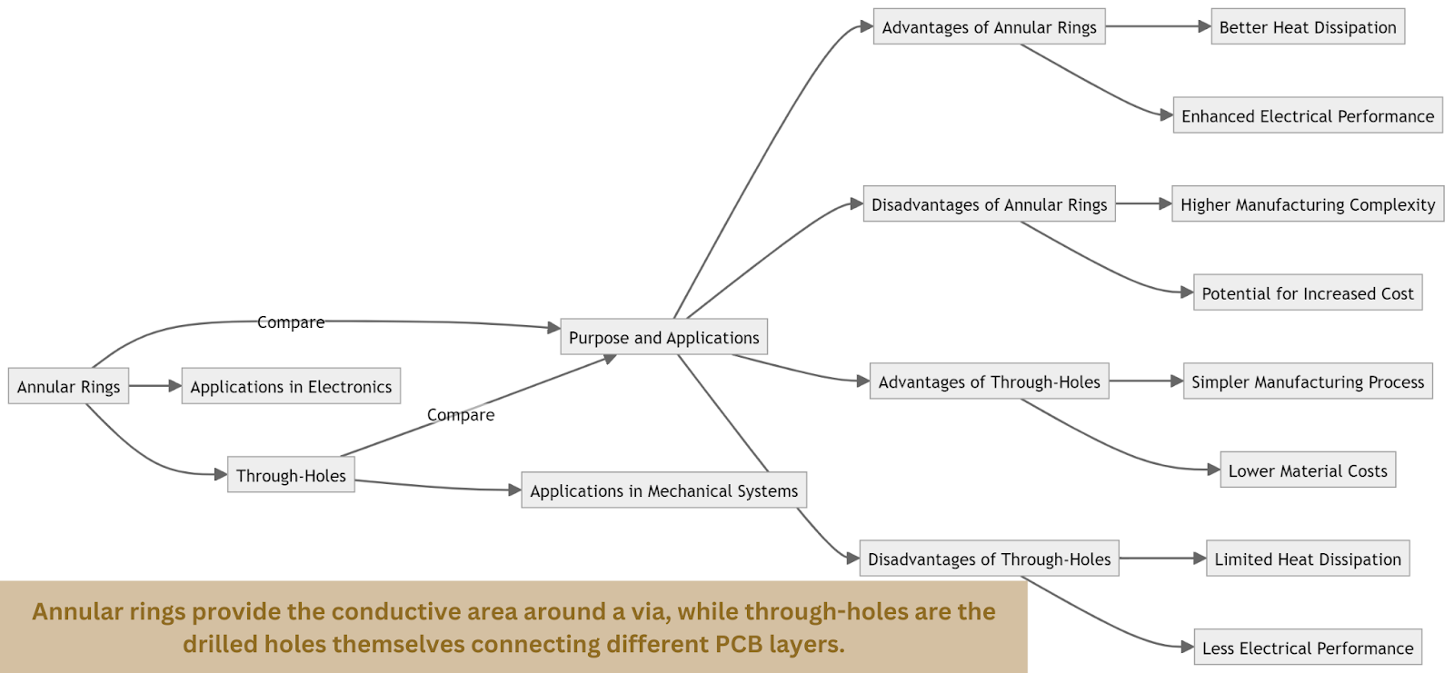
Annular Rings vs. Through-Holes
Understanding Teardrop Annular Rings
Teardrop annular rings are specialised pads that connect pads to traces or vias with a tapering, teardrop-shaped shape. They are employed to increase solder joint dependability and mechanical strength.
Conclusion
Mechanical strength and dependable electrical connections in PCB design depend on the right application of annular rings. Manufacturers are required to follow IPC guidelines mainly regarding the sizing of the rings to ensure durability of the electronic devices. Above all, consult the professionals who have experience on sophisticated PCB design processes in order to get the best outcomes.
Table of Contents
Understanding Annular Rings
How To Calculate the Size of Annular Rings
Importance of Annular Ring Size
Annular Rings and Vias
Understanding Teardrop Pads
The Structure of a PCB Annular Ring
Role of the Annular Ring structure in the functionality of PCBs
How To Get a Correct Annular Ring Size
Industry standards and best practices:
What Are The Minimum Annular Ring Requirements
Annular Rings vs. Through-Holes
Frequently Asked Questions
What is an annular ring in PCB design?
An annular ring in PCB design is the ring-shaped area of conductive material surrounding a drilled hole (via). Its role is to ensure reliable electrical connections between different PCB layers and to provide mechanical support for components and vias.
Why is the size of the annular ring important?
An annular ring's size is important because it provides sturdy mechanical support and dependable electrical connections. Appropriately dimensioned rings improve overall PCB performance and reliability by preventing weak solder junctions and lowering the chance of fractures.
How do you calculate the annular ring size?
To find the annular ring size, use the following calculations:
- Measure the diameter of the hole (via).
- Find the diameter of the pad surrounding the hole.
- Annular Ring Width = (Pad Diameter - Hole Diameter) / 2 is the formula to use.
What are common issues with annular rings?
- Inadequate Ring Size: Soldering problems and poor electrical connections can result from small rings. Make sure that the rings are at least a certain size.
- Misalignment: A misaligned hole might make the ring's effective width smaller. Make exact alignment and drilling decisions.
- Plating Defects: Unreliable connections might result from partial or uneven plating. Adhere to the recommended plating procedures and quality controls.
What is a teardrop pad in PCB design?
In PCB design, a teardrop pad is a pad that seamlessly flows from a trace or via to another pad with a tapered, teardrop-like shape. By more equally distributing mechanical stress, this design lowers the possibility of fractures or weak spots. To strengthen the connection, teardrop cushions are frequently utilised with annular rings. By offering a gentle transition, the teardrop form supports the annular ring and enhances its mechanical and electrical reliability.
%20(1).jpg)
