Regarding electronics, voltage references are absolutely essential for the stable and precise running of circuits after PCB assembly. By providing standards for operating situations in different components, voltage references—like VDD and VCC—allow exact control and functionality.
Among the most often used voltage references in electric circuits are VDD and VCC. For digital circuits, VDD usually signifies the positive supply voltage; for analog and bipolar junction transistor (BJT) circuits, VCC describes the positive supply voltage in analog circuits.
Design and troubleshooting of circuits depend on an awareness of these words since they affect the stability and performance of electronic devices. While VCC is often used in analog circuits, power supply, and BJT setups, VDD is routinely employed in contexts including digital logic circuits, microcontrollers, and CMOS technologies.
Read on to have a comprehensive knowledge about VDD and VCC.
Key Highlights
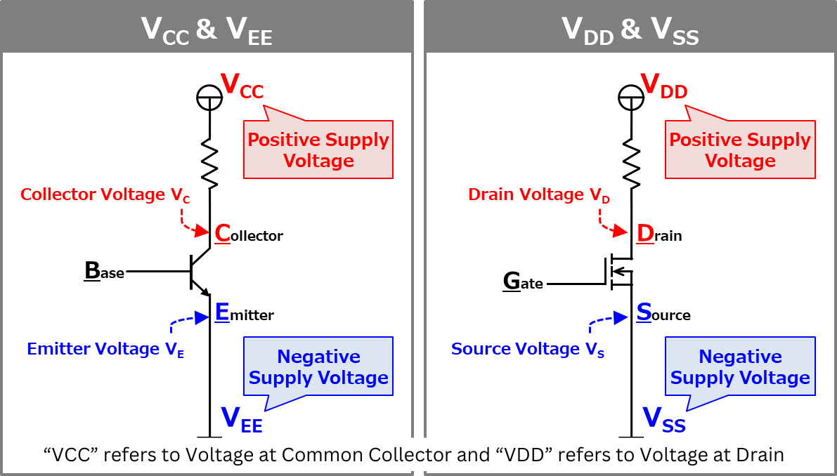
- VCC stands for "Voltage at the Common Collector" and is typically the positive supply voltage for BJT circuits.
- VDD Refers to "Voltage at the Drain" and is used as the positive supply voltage in digital and MOSFET circuits.
- Due to its fit for linear signal amplification, VCC is recommended in terms of usage context in analog application while VDD fits well for digital electronics due to low power consumption.
- You must place decoupling capacitors close to the power pins, use ground planes, and keep power supply traces short while using VDD and VSS.
- In case you detect any issues with the VDD or VSS, you must look for any signs like unexpected resets, use a multimeter to measure continuity, inspect PCB layout, and check for any ground loops.
Voltage References In Different Types of Circuits: VCC, VDD, VEE, VSS, and GND
Fundamental in nature, voltage references give consistent supply voltages necessary for the proper operation of many PCB components. The main voltage references are succinctly explained here in clear language:
- VCC: Stands for "Voltage at the Common Collector" and is typically the positive supply voltage for bipolar junction transistor (BJT) circuits.
- VDD: Refers to "Voltage at the Drain" and is used as the positive supply voltage in digital and MOSFET (Metal-Oxide-Semiconductor Field-Effect Transistor) circuits.
- VEE: Represents the negative supply voltage in BJT circuits, often associated with the emitter terminal.
- VSS: Denotes "Voltage at the Source" and is commonly the ground or negative supply voltage in MOSFET circuits.
- GND: Short for "Ground," this is the reference point for all voltages within the circuit, typically considered as 0 volts.
Historically, these words changed along with semiconductor technology. While VDD and VSS became common with the advent of MOSFET technology, VCC and VEE were set during the time when BJTs were common. These voltage references provide consistency in circuit design, therefore enabling engineers to efficiently apply power sources over several kinds of circuits.
Here’s a simple diagram to illustrate these relationships:
Practical Applications of VCC and VDD
Powering a variety of devices and circuits, VCC and VDD are absolutely essential for their stability and performance. Analog circuits and devices including bipolar junction transistors (BJTs) routinely use VCC. Among examples are power amplifiers, radio frequency circuits, and operational amplifiers. VCC supplies the required positive supply voltage to the collector of BJTs in certain applications, therefore allowing the correct operation of these parts.
Conversely, VDD is typically applied in digital circuits and devices running MOSFET technology. Microcontrollers, microprocessors, memory chips, and digital signal processors are few examples here. Crucially for the operation of digital logic gates and other digital circuit elements, VDD provides the positive voltage to MOSFET's drain terminal.
The whole operation of electronic devices depends on VCC and VDD playing a basic power role for several components. VCC guarantees that analog circuits preserve their necessary voltage levels for signal amplification and processing; VDD is needed for the logical operations and data processing chores carried out by digital circuitry.
In practical terms, VCC is essential in devices like audio amplification, where clear sound output depends on steady voltage. In computer devices, where correct data processing and memory operations depend on constant voltage levels, VDD is absolutely essential.
Types of Grounding in Electronics
Crucially important in electrical design, grounding guarantees circuit stability and helps to prevent noise and interference. Grounding comes in several forms, each with specific uses:
- Signal Ground: This type of grounding is used to reference and stabilise signal voltages within a circuit. Signal ground is crucial in ensuring accurate signal transmission and minimising noise in analog and digital circuits.
- Power Ground: Also known as power return ground, it is used to complete the return path for power supply currents. Proper power grounding is vital for the efficient operation of power circuits and to prevent voltage drops.
- Chassis Ground: This is the grounding connected to the physical enclosure or chassis of a device. Chassis ground provides a safety path for fault currents, protecting users from electric shock and reducing electromagnetic interference (EMI).
Reducing noise and interference depends on proper grounding, which also helps sensitive electronic components to function as intended. Common methods to attain good grounding in PCB layers are separating signal and power grounds, employing a single ground point (star grounding), and ground plane use.
For audio equipment, for instance, good grounding is crucial to stop hum and noise. Multiple grounding points and ground planes help to guarantee steady operation and signal integrity in computer motherboards. Chances grounding helps automotive electronics ensure safety and lower EMI.
Comparing VCC and VDD
Two fundamental voltage references in electronics, VCC and VDD have different uses depending on the kind of circuit they run over.
Due to its fit for linear signal amplification, VCC is recommended in terms of usage context in analog applications like RF transmitters and audio amplifiers when BJTs are used. Digital electronics including microcontrollers, CPUs, and memory devices prefer VDD since MOSFETs with their low power consumption and high switching rates are utilised there.
In analog circuits, typical voltage values for VCC vary from 5V to 15V; in digital circuits, VDD values typically range from 1.8V to 5V, therefore reflecting the reduced power requirements of contemporary digital components.
Using VCC and VDD in Microcontrollers
By supplying the required supply voltages for their internal circuitry, VCC and VDD are absolutely vital for microcontroller operation. Their voltage references guarantee proper and effective operation of the components of the microcontroller.
Microcontroller families using VCC and VDD include the Microchip PIC series and the Atmel AVR series. While VDD drives the core digital logic, the AVR microcontrollers—including the ATmega328—often use VCC for their analog-to--digital converters (ADCs) and other analog peripherals. Likewise, the PIC microcontrollers—including PIC16F877A—use VCC for digital logic operations and VCC for analog components.
Microcontroller performance and capability are strongly influenced by VCC and VDD. Reliable microcontroller operation depends on stable and accurate VCC and VDD voltages, therefore affecting parameters including processing speed, peripheral performance, and general system stability.
To reduce noise and interference, best practices for using VCC and VDD in microcontroller-based projects include guaranteeing appropriate decoupling with capacitors near the microcontroller pins, maintaining clean and reliable power supply lines, and separating analog and digital grounds.
Key Technical Differences and Implications: VDD vs VSS
Particularly in the context of MOSFET-based designs, VDD and VSS are absolutely essential voltage references in electronic circuits. VDD is usually coupled to the drain of an n-channel MOSFET, required for digital logic operations. Conversely, VSS is the ground or negative supply voltage, usually coupled to the MOSFET's source and provides the circuit's reference point.
Their functions define their fundamental technical differences: VDD produces the positive voltage needed to run the circuit, while VSS offers the return channel for the current, therefore preserving reference and circuit stability. In electronic design, this difference is rather important. Digital and analog component proper operation depends on VDD, which also affects aspects including switching speed and logic levels.
In circuits such as digital signal processors (DSPs) and microprocessors, VDD and VSS choice is crucial. In a CMOS inverter, for example, VDD supplies the power needed for the transistor to operate; VSS guarantees the transistors' appropriate switching by acting as the ground reference.
Typical VDD values fall between 1.8V and 5V; VSS is typically 0V (ground). Comparisons of performance show that eliminating noise, obtaining high-speed performance, and guaranteeing dependable operation in complicated electronic systems depend on consistent VDD and VSS voltages.
Core Concepts: VDD and VSS
Particularly in electrical circuits incorporating MOSFETs, VDD and VSS are basic voltage references absolutely essential for their operation.
VDD supplies the required energy in transistor operation to run the logic and analog circuits. VDD energises the transistor in MOSFETs, therefore allowing current flow from the drain to the source when the gate voltage is applied. Acting as the reference point, VSS completes the circuit and guarantees a stable return path for current, therefore ensuring the transistor's correct operation.
By controlling the voltage levels at which transistors turn on and off, VDD and VSS dramatically impact circuit behaviour, therefore influencing the general speed and efficiency of the circuit. In digital circuits, for instance, a greater VDD could boost transistor switching speed but might also cause more heat dissipation and power consumption. On the other hand, VSS guarantees that every component has a shared reference point—necessary for precise signal processing and noise reduction.
Additional Voltage References and Transistor Configurations
Often used voltage references besides VDD and VSS are VBB, VCC, and VEE. VBB in bipolar junction transistor (BJT) circuits refers to the base bias voltage. Usually connected to the collector, VCC stands for the positive supply voltage in BJT setups; VEE stands for the negative supply voltage, typically attached to the emitter.
Unique voltage needs abound in transistor designs including common-emitter, common-collector, and common-base for BJTs and common-source, common-drain, and common-gate for MOSFETs. VCC drives the collector in a common-emitter BJT arrangement; VEE may be utilised for the emitter; VBB biases the base to enable switching and amplification. VDD feeds the drain in a common-source MOSFET arrangement; VSS provides the source voltage reference.
These configurations affect circuit design by determining the biassing conditions required for best transistor functioning and the power supply layouts. The desired performance, stability, and efficiency of the circuits are guaranteed by appropriate choosing and implementation of these voltage references.
An operational amplifier (op-amp) circuit might, for instance, use VCC and VEE to provide positive and negative supply voltages, therefore allowing the op-amp to efficiently manage both positive and negative input signals. Usually running the CMOS gates with VDD and VSS, a digital logic circuit guarantees consistent switching between logical levels.
Here’s a table summarising the usage of various voltage references:
Relationship Between VDD and VSS
Particularly in those employing MOSFETs and digital logic, VDD and VSS are interdependent voltage references that are absolutely vital for the operation of electronic circuits. Their mutual dependency guarantees that current has a return channel and that parts get the required power for functioning, hence preserving circuit stability.
VDD provides the voltage to the drain terminal in a conventional MOSFET-based circuit, therefore supplying the energy required for the transistor to run. Linked to the source terminal, VSS serves as the reference point enabling current to pass across the transistor under applied gate voltage.
Maintaining the right running conditions of the components depends on the collaboration between VDD and VSS. While VSS must offer a steady ground reference to prevent noise and guarantee correct signal processing, VDD must be reliable and sufficient to run the components. Making sure VDD and VSS are correctly separated with capacitors will help to filter noise and produce constant voltage levels.
Case Studies
- CMOS Inverter
- Whereas VSS provides ground for the n-channel MOSFET in a CMOS inverter, VDD drives the p-channel MOSFET. The p-channel MOSFET is on low input, raising the output to VDD. The n-channel MOSFET is active when high input levels drag the output low to VSS. This complementing action between VDD and VSS guarantees effective logic level switching.
- Microcontroller
- VDD drives the fundamental digital logic circuitry in microcontrollers such as the ATmega328; VSS offers the ground reference. While VSS guarantees constant operation by grounding the system and lowering noise, VDD's stability is essential for the correct running of the CPU and its peripherals.
- Operational Amplifier
- Positive and negative supply voltages in an op-amp circuit are derived from VDD and VSS correspondingly. By allowing the op-amp to manage both positive and negative input signals, this twin supply arrangement increases its adaptability in analog signal processing uses.
Recent Innovations in Voltage Reference Technology
Voltage reference technology has lately made major progress that greatly enhances circuit efficiency and performance. Electronic circuits' stability and precision have been improved by innovations including temperature-compensated references and ultra-low noise voltage references. These developments guarantee constant voltage levels for components, so lowering mistakes and increasing general dependability.
The creation of bandgap reference circuits—which offer mostly independent of temperature and supply fluctuations and reliable output voltages—is one noteworthy breakthrough. Precision analog uses of these circuits abound in data converters and instrumentation amplifiers. Another recent development enabling more compact and effective designs is the inclusion of voltage references inside semiconductor devices.
For high-accuracy measurement systems, Texas Instruments' REF70 series provides low-drift voltage references with high-precision and noise as low as 1.4 µVrms. Furthermore adding freedom to circuit design are digital voltage references, which can be configured to offer different output voltages.
Modern semiconductor materials and quantum-dot-based references could transform voltage reference technology and offer even more stability and precision for next-generation electronic systems.
Advances in VSS Grounding Techniques
Particularly for VSS, recent developments in grounding methods have greatly improved circuit stability and noise lowering. Minimising interference, guaranteeing signal integrity, and preserving general circuit performance depend on proper grounding. The growing complexity of electronic circuits and the necessity of more dependability and precision drive innovations in grounding techniques.
Enhanced Stability and Noise Reduction
Modern grounding methods centre on lowering ground loops, eliminating electromagnetic interference (EMI), and guaranteeing a low-impedance link to ground. More advanced techniques now complement approaches such multi-point grounding and star grounding. For the PCB fabrication process, for instance, ground planes are now normal procedure.
New Grounding Methods
Using hybrid grounding schemes—that is, combining many grounding strategies to maximise performance—is one recent development. This includes isolating noise-sensitive components by combining ground planes with segmented grounds for separate circuit parts, hence lowering cross-talk. Furthermore showing promise in improving conductivity and lowering thermal noise are the use of innovative materials and conductive polymers for grounding.
Active grounding is another developing technique. This strategy is especially helpful in high-frequency PCB uses when conventional grounding techniques might not be sufficient.
Industry Insights
Professionals in the field stress the need for ongoing innovation in grounding methods. Experts emphasise that improved grounding techniques are absolutely essential as electronic devices get more sophisticated and small. Future developments will probably centre on adaptive grounding methods able to react to real-time changes in circuit conditions.
Future Prospects
Grounding methods' future looks to be marked by major developments, such as quantum grounding. It uses quantum events to reach near-perfect grounding. Moreover, there is the integration of AI-driven grounding management systems that dynamically optimise grounding lines in real-time. These technologies should improve circuit stability, lower noise, and guarantee dependability.
Practical Considerations and Challenges
Circuit use of VDD and VSS has numerous difficulties mostly related to noise, voltage stability, and power dissipation. Circuit performance depends on these voltage references preserving their intended levels free from interference.
Common Challenges
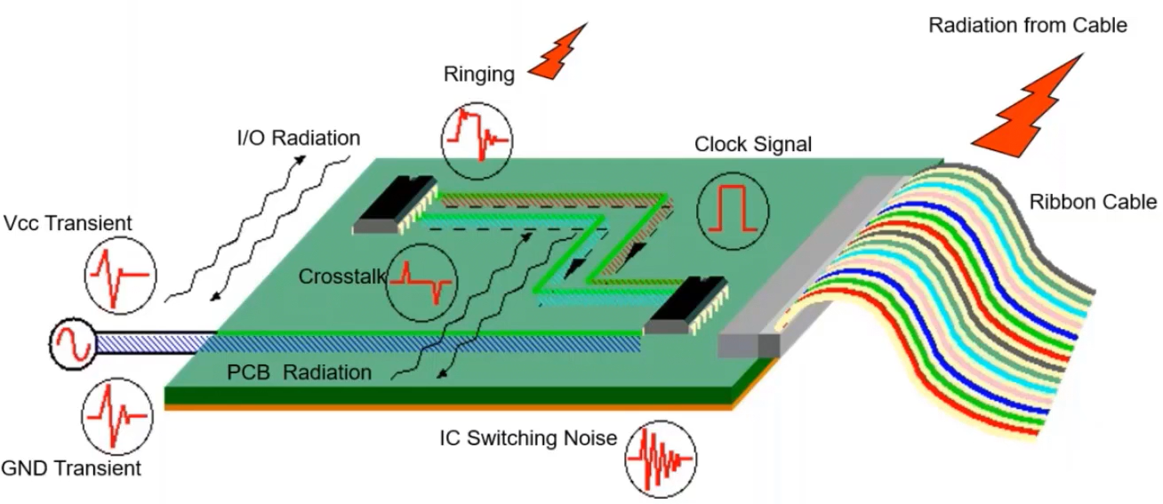
- Noise and Interference: Noise from other components can couple into the power supply lines, affecting the stability of VDD and VSS.
- Voltage Drops: Long traces on PCBs can cause voltage drops, impacting the reliability of VDD and VSS.
- Heat Dissipation: High currents can lead to heat generation, affecting the integrity of VDD and VSS.
Practical Tips
- Decoupling Capacitors: Place decoupling capacitors close to the power pins of ICs to filter out noise and provide a stable VDD and VSS.
- Ground Planes: Use ground planes to minimise impedance and reduce noise coupling into VSS.
- Short Traces: Keep power supply traces short and wide to reduce voltage drops and improve current handling.
Real-World Problems and Solutions
- Problem: A microcontroller resets randomly due to voltage spikes on VDD.some text
- Solution: Add a larger decoupling capacitor (e.g., 100µF) near the microcontroller to smooth out voltage fluctuations.
- Problem: Analog signal noise in mixed-signal circuits.some text
- Solution: Separate analog and digital grounds, connecting them at a single point to reduce interference.
Best Practices
- Power Integrity Analysis: Perform simulations to ensure VDD and VSS maintain their stability under different load conditions.
- Thermal Management: Implement adequate cooling solutions, such as heat sinks, to manage heat dissipation.
What are the Common Issues with VDD
VDD, the positive supply voltage in many circuits, can encounter several issues that impact circuit performance and reliability.
Frequent Issues
- Voltage Fluctuations: Inconsistent VDD levels can cause instability in circuit operation.
- Noise and Ripple: High-frequency noise or ripple on VDD can interfere with sensitive components.
- Overvoltage and Undervoltage: VDD levels exceeding or falling below the required voltage can damage components or lead to malfunction.
- Power Supply Drop: Voltage drops due to long PCB traces or insufficient power supply capacity.
Causes and Prevention
- Voltage Fluctuations: Often caused by load variations or inadequate power supply regulation. Prevent by using voltage regulators and ensuring the power supply can handle the load.
- Noise and Ripple: Caused by switching power supplies or external interference. Minimise by using decoupling capacitors, ferrite beads, and proper multilayer PCB design techniques.
- Overvoltage and Undervoltage: Result from power supply malfunctions or improper settings. Use voltage protection circuits like Zener diodes or TVS diodes.
- Power Supply Drop: Due to high resistance in long traces. Design PCBs with short, wide traces for power lines and use low-dropout regulators.
Troubleshooting Tips
- Measure VDD at Various Points: Use an oscilloscope to check for voltage consistency and noise.
- Check Power Supply Ratings: Ensure the power supply meets the circuit’s voltage and current requirements.
- Inspect PCB Layout: Verify that power traces are adequate and decoupling capacitors are correctly placed.
Examples of Common Problems
- Microcontroller Resetting: Caused by VDD drops during high current draw. Solution: Add a bulk capacitor close to the microcontroller.
- Analog Signal Distortion: Due to VDD noise. Solution: Use a linear regulator to provide a cleaner VDD.
Troubleshooting VSS Problems
VSS, often serving as the ground reference in circuits, is crucial for stable operation. Issues with VSS can cause significant problems. Here's a step-by-step guide to troubleshooting VSS issues.
Step-by-Step Guide
- Identify Symptoms: Look for signs like unexpected resets, noise in analog signals, or inconsistent digital logic levels.
- Measure VSS: Use a multimeter to check for continuity between VSS and the ground plane. Ensure there’s no significant resistance.
- Inspect PCB Layout: Verify the integrity of ground connections, ensuring no broken traces or cold solder joints.
- Check for Ground Loops: Ensure that multiple ground paths don’t create loops, which can introduce noise.
- Analyse Current Paths: Ensure high-current paths don’t interfere with sensitive signals.
Common Symptoms and Causes
- Noise and Interference: Often caused by poor grounding or ground loops.
- Inconsistent Logic Levels: Can be due to voltage drops in VSS traces.
- Unexpected Resets: Typically caused by ground bounce or poor grounding.
Practical Solutions and Preventive Measures
- Use Ground Planes: Implementing ground planes can minimise impedance and noise.
- Short, Wide Traces: Ensure VSS traces are short and wide to handle current without significant voltage drop.
- Decoupling Capacitors: Place capacitors close to VSS pins of ICs to filter out noise.
- Single Point Grounding: Use a star grounding scheme to prevent ground loops.
Examples
- Case of Analog Noise: An audio amplifier exhibited noise due to a ground loop. Solution: Re-routed ground paths to a single point, eliminating the loop and noise.
- Microcontroller Reset Issue: A microcontroller reset intermittently due to ground bounce. Solution: Added more decoupling capacitors and improved ground plane connectivity.
Conclusion
Designing stable and effective systems depends on a knowledge of the roles and variations between VDD and VCC in electronic circuits. Important themes cover the need of appropriate voltage references, sophisticated grounding techniques, and efficient VDD and VSS troubleshooting approaches. Knowing this guarantees consistent circuit performance. One must be educated about voltage reference technology and best practices as electronics develop.
Table of Contents
Voltage References In Different Types of Circuits: VCC, VDD, VEE, VSS, and GND
Practical Applications of VCC and VDD
Types of Grounding in Electronics
Comparing VCC and VDD
Using VCC and VDD in Microcontrollers
Key Technical Differences and Implications: VDD vs VSS
Core Concepts: VDD and VSS
Additional Voltage References and Transistor Configurations
Relationship Between VDD and VSS
Recent Innovations in Voltage Reference Technology
Advances in VSS Grounding Techniques
What are the Common Issues with VDD
Troubleshooting VSS Problems
FAQ's
What are VCC and VDD?
In electronics, VCC and VDD are fundamental voltage references. Usually the positive supply voltage in bipolar junction transistors (BJT), VCC is "Voltage at the Common Collector". It offers BJTs' collector terminal the required power. Conversely, VDD, or "Voltage at the Drain," is the positive supply voltage in metal-oxide-semiconductor field-effect transistor (MOSFET) circuits, especially in digital and CMOS uses. Providing the energy needed for circuit operation, both VCC and VDD are essential for guaranteeing the correct running of their respective components.
Why are VDD and VCC important in electronics?
In electronics, VDD and VCC are absolutely important since they provide the required power to different circuit components, therefore guaranteeing their appropriate operation. For digital circuits, VDD guarantees consistent digital logic operations and serves as the positive voltage for MOSFETs. For analog and BJT circuits, VCC provides the positive voltage, therefore permitting exact signal amplification and processing. Maintaining circuit stability, performance, and efficiency depends on a knowledge of and appropriate application for these voltage references. Correct VDD and VCC levels guarantee the general dependability of electronic equipment and systems, help to prevent failures, and lower noise levels.
How do VDD and VCC differ from each other?
Mostly in their applications and the kinds of components they run on, VDD and VCC vary. Digital circuits and MOSFET-based devices employ VDD, the positive supply voltage. Commonly found in digital logic circuits, microcontrollers, and memory chips, MOSFETs run their drain terminal under power. On analog circuits and BJT-based components, VCC is the positive supply voltage. It drives BJTs, which are utilised in analog circuits including amplifiers and RF circuits, their collector terminal.
What are common issues with VDD and VSS, and how can they be resolved?
While VSS problems usually entail noise, ground loops, and voltage drops, common VDD problems include voltage fluctuations, noise, and overvoltage or undervoltage circumstances. In circuits these problems can lead to instability, signal interference, and malfunction. Use voltage regulators to preserve steady voltage, decoupling capacitors to filter noise, and guarantee appropriate PCB architecture to reduce voltage drops in order to tackle VDD problems. Use ground planes to lower impedance, steer clear of ground loops using a single-point grounding system, and guarantee short, wide traces for strong grounding for VSS.
What advancements have been made in voltage reference technology recently?
Voltage reference technology has recently advanced with an eye toward stability, accuracy, and energy economy. Electronic circuits now operate far better thanks in great part to innovations including temperature-compensated references and ultra-low noise voltage references. For precision analog uses, technologies such as bandgap reference circuits offer steady output voltages independent of temperature and supply fluctuations. Small and effective solutions are provided by integrated voltage references found in semiconductor devices.