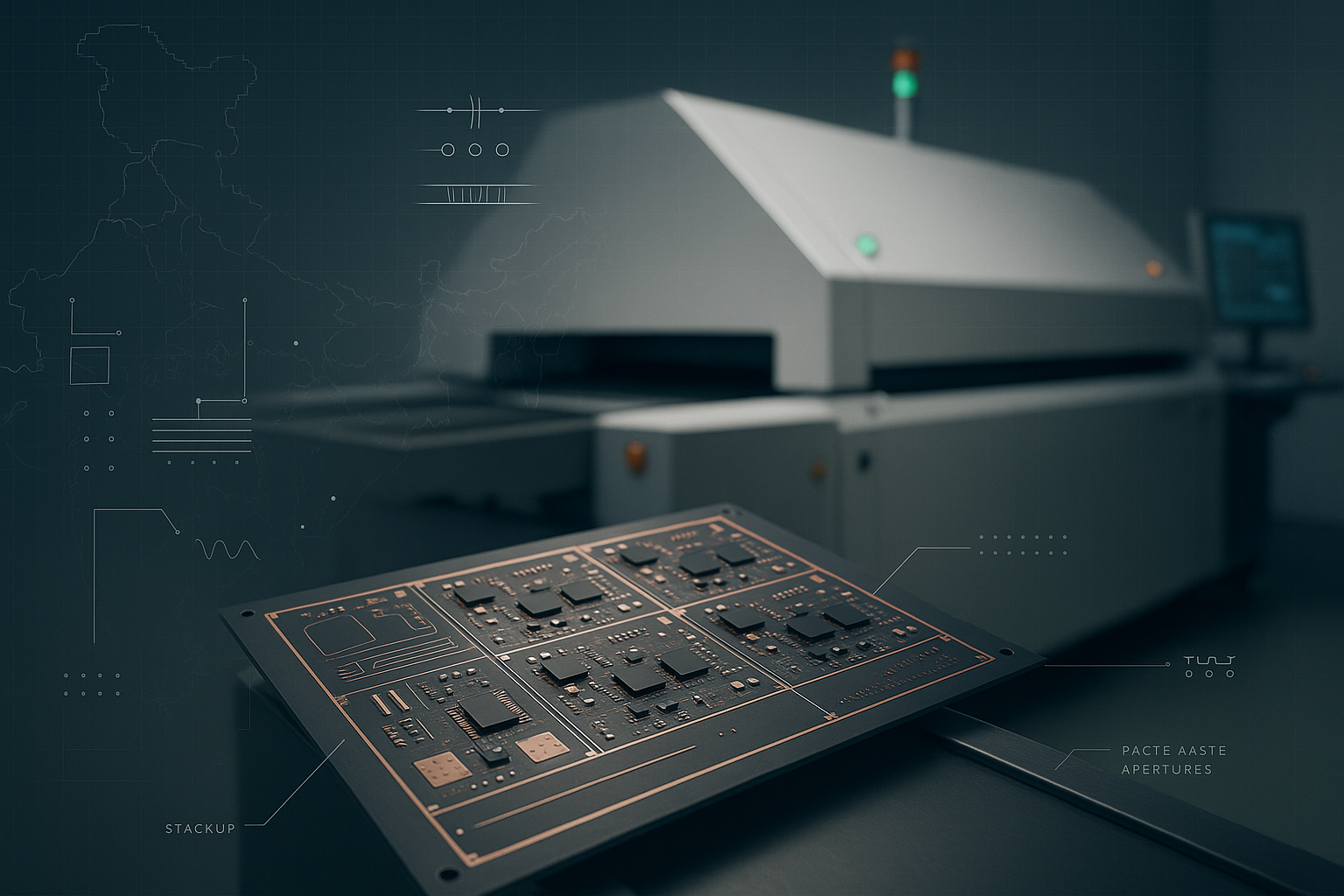
Overview of PCB Layout
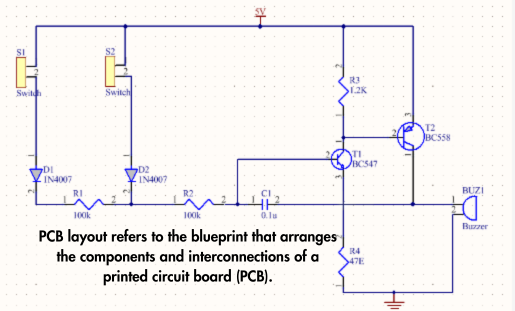
PCB layout refers to the blueprint that arranges the components and interconnections of a printed circuit board (PCB). It is mainly prepared to guide the manufacturers to transform the design into a functional board by improving the placement of PCB components. As a result, the trace length and routing can be optimised to minimise signal issues.
Some of the most common materials used for PCB layout construction are:
- FR-4: This is the most commonly used PCB material and is made of fiberglass-reinforced epoxy resin. It is mainly applicable to cases where good thermal stability and mechanical strength are required.
- I-Speed: As the name suggests, it is a high-speed and low-loss material that is a perfect match for high-frequency applications.
- Rogers: They are a set of top-performance PCB materials that are well-known for thermal management.
- Polyimide: They are mainly used in flex PCBs due to their high-temperature resistance and compactness features.
Key Highlights
- PCB layout refers to the blueprint that arranges the components and interconnections of a printed circuit board (PCB).
- While placing the components on the PCB layout, make sure that the trace lengths are minimal and avoid sharp turns.
- There are various steps to design a PCB like schematic design, component placement, trace routing, and Gerber file generation.
- PCB layouts are mainly used in radio, microwave, automotive, aerospace, and medical devices to improve their durability, reliability, signal strength, and performance.
- Companies must ensure proper cleaning and inspection to maintain the PCBs without any defects and may require specialised tools for their repair.
- Some of the main advantages of PCB layouts are durability, reliability, thermal management, early detection of faults, and encouragement to try new designs.
- The main challenges during the PCB layout process are the demand for miniaturisation, high-speed signal transmission, specialised equipments, and higher costs.
- PCB layout techniques are advancing rapidly to meet the growing needs of future technologies like 5G and IoT.
PCB Layout Design Considerations
While designing a PCB layout, there are several considerations to keep in mind. Have a look at them:
- Place the ground and power planes on the outer layers of the stack-up to cover traces like a sandwich. This improves the signal strength of the device.
- Arrange the components in such a way that the trace lengths are minimal.
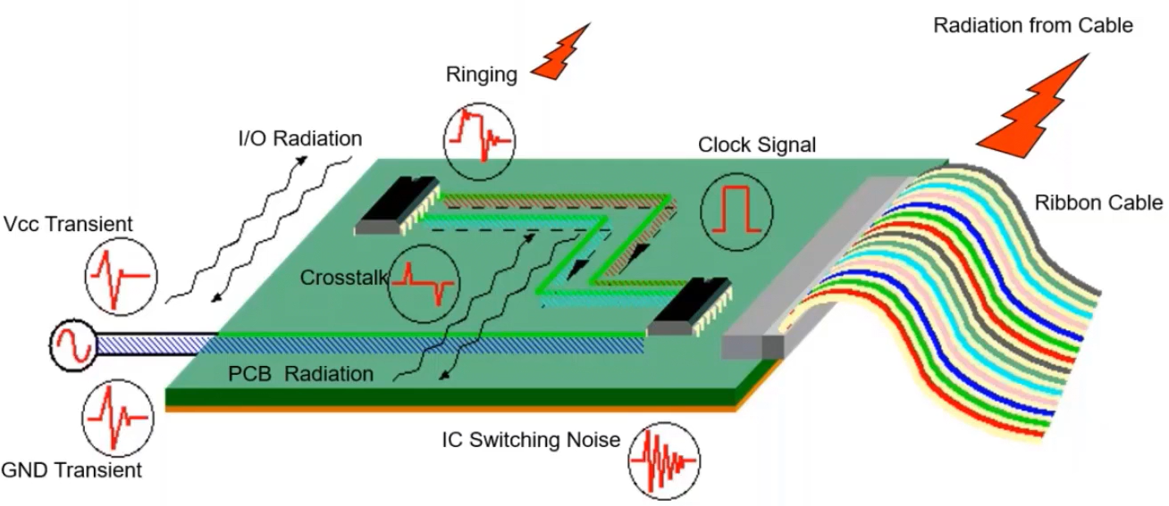
- Avoid sharp corners and right angles in signal routing to avoid reflections.
- Make sure that there is sufficient space between components and traces to allow for proper airflow for smoother heat dissipation. On top of that, manufacturers can also consider the use of heat sinks for better thermal management.
Designing a PCB Layout
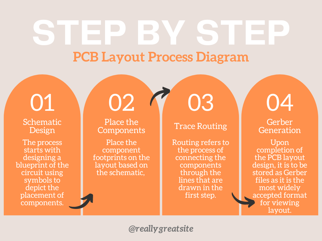
Designing a PCB layout is a crucial process that requires in-depth planning and proper execution. Here is a step-by-step process flow for creating a PCB layout:
1. Schematic Design
The process starts with designing a blueprint of the circuit using symbols to depict the placement of components. This serves as the baseline of the entire process. Designers are required to draw through the components to represent the interconnections of the layout. Software like Altium and Allergo can make the entire process easier by allowing users to capture schematics of any complexity without any complexity.
2. Place the components
Now, place the component footprints on the layout based on the schematic, keeping in mind the electrical requirements of the board. Many manufacturers use CAD software to automatically place the components and route the traces in accordance with the design. Such tools include advanced features to identify any issues in the design.
3. Route the Traces
Routing refers to the process of connecting the components through the lines that are drawn in the first step. These traces conduct electricity throughout the devices and they are mainly made of copper traces. Designers must try as much as possible to minimise the track length and avoid sharp bends to avoid signal degradation.
4. Gerber Generation
Upon completion of the PCB layout design, it is to be stored as Gerber files as it is the most widely accepted format for viewing layout. Gerber files contain 2D artwork data that indicates where the manufacturing processes like PCB etching, solder mask application, etc. should occur on the physical PCB. These files are used to create photomasks that will be used to transfer the circuit patterns onto the PCB surface.
After this, copper layers are laminated to a base PCB material that will be created using fibreglass or Teflon to which a light-sensitive photoresist material is applied. Now, the photomask is placed over the PCB and is exposed to UV light. The exposed part is then developed as a PCB.
PCB Manufacturing
PCB layout is the first step towards PCB manufacturing. It serves as the base upon which the entire functional board is created. Have a look at the next stages of PCB manufacturing:
1. Surface Preparation
PCB etching is done through chemical solutions or plasma treatment to harden the surface. In the case of Teflon PCBs, the surface is first soaked in a sodium-based solution to remove the fluorine.
2. Teflon Coating
Teflon is coated to the PCB surface to equip it with superior dielectric properties to make it suitable for high-frequency applications. Teflon coatings are applied to prepare the surface with excellent dielectric properties for the copper cladding and lamination process. On top of that, Teflon can improve chemical resistance by protecting the device from corrosion.
3. Copper Cladding
When the surface is hard enough, copper foils are laminated to creative conductive paths. It is always recommended to use high-tensile strength copper as it can prevent issues like barrel crackdowns.
4. Drilling
Now, it's time to drill the PCB to create the necessary vias and holes for component placement. The entire drilling process is typically done through a computer-controlled drilling machine with proper inspection.
5. Lamination
Both inner and outer PCB layers, including copper cladding and Teflon coating, are stacked together using metal clamps on a special press table. Then, it is moved to the laminating press to apply heat and pressure to fuse the PCB layers together.
6. Outer Layer Imaging and Etching
The outer copper layers are patterned using a photoresist and then etched to create the final circuit traces. If needed, manufacturers can apply surface finishes like ENIG to the PCB.
7. Inspection and Testing
Quality control is done through techniques like Automated Optical Inspection (AOI) that compares the PCB to the design files to identify any defects. Apart from that, a comprehensive visual test is done to make sure that the board's functioning is up to the standards.
PCB Layout Applications
PCB layouts play a crucial role in the performance of many electronic devices. Check out how it is used in various situations:
1. Radio and Microwave Systems
High-frequency devices like radio and microwave systems require a well-structured PCB layout to function. Here is how it helps:
- Signal Integrity: Optimisation of trace routing through PCB layout helps to maintain signal strength. Manufacturers can use advanced techniques like coplanar waveguides to prevent the chances of reflections, crosstalks, etc.
- Noise Reduction: Strategic component placement helps to isolate sensitive analogue and RF circuits from digital noise sources.
2. Aerospace and Automotive Devices
Devices in sectors like aerospace and automotive that require reliability to withstand harsh environments can benefit greatly from PCB layouts. See how:
- Thermal Resistance: Placement of components with sufficient spaces in between ensures efficient heat dissipation.
- Reliability: With the usage of PCB layout techniques like reinforced plated-through holes, the mechanical strength of the devices could be maintained to a certain extent. Apart from that, manufacturers can use additional coating like ENIG PCBs to provide additional protection to devices from harsh environments.
3. Medical devices and Industrial control systems
Apart from normal devices, PCB layouts are significant for many specialised applications too. Check out how:
- Performance: Efficient PCB layout structure can minimise parasitic effects to improve the responsiveness of devices, especially medical sensors. Moreover, careful race routing can provide a low-impedance path for high-frequency signals to maintain signal strength.
- Durability: Conformal coatings can be done to protect the PCB from moisture, chemicals, or other contaminants.
PCB Layout Maintenance and Repair
Just like the above-mentioned steps, proper cleaning is a crucial activity to ensure the lifetime of a PCB. For instance, the soldering process leaves something called flux residue. Even though flux helps in the soldering process, if not cleaned after assembly, it can degrade the surface insulation resistance and can cause serious problems like long stabilisation times.
Therefore, to ensure proper cleaning, consider using an ultrasonic bath. Once the board is cleaned, the board should be dried, preferably through air-drying to remove any residual moisture that could create short circuits. Above all these, conduct manual inspections regularly to detect any dust or contaminants. Make sure that the storage environment is always neat.
When it comes to repairing, it is recommended to use specialised tools such as soldering irons, precision tweezers, etc., to optimise the process. One simple advice during repair is to always try to avoid direct contact with the board to avoid contaminants. If the situation demands direct contact, ensure that the staff wear neat gloves.
Advantages Of Using PCB Layout
Have a look at some of the key advantages of using PCB layouts:
1. Durability and Reliability
Standard PCB layout measures help the manufacturers address the challenges that may affect the device in the future. For instance, noble metals like gold or palladium instead of base metals like copper for surfaces that are more vulnerable to corrosion. As a result, the lifespan of the device gets longer and it works reliably.
2. Thermal Management
The strategic placement of components with sufficient gaps ensures that there is enough space to allow for the transfer of heat. It prevents local hotspots and saves the device components from cracks during high-temperature processes.
3. Signal Integrity
Electromagnetic interfaces and cross-talks could be avoided to a great extent through careful trace routing. Moreover, it can prevent sharp turns in the routes which further contribute to the signal strength of the device.
4. Early Detection and Fixing
PCB layout is all about planning ahead to improve the functioning of PCB. CAD software tools can help manufacturers detect any issues earlier and fix them on time before things go out of hand.
5. Try Innovation
The PCB layout process gives space to a virtual testing environment which encourages designers to try out new experimental designs as there is not much risk involved.
PCB Layout Challenges
Despite these attractive advantages, there are many challenges to overcome while creating a PCB layout. Check out them:
1. Demand for Miniaturisation
Nowadays, the demand for compact and lightweight features is larger than ever before in the market. Therefore, manufacturers are under pressure to accommodate more components in a limited space which may increase the complexity of routing traces.
2. High-Speed Signal Transmission
Manufacturing of advanced high-speed circuits is getting tougher due to many factors like trace impedance, length matching, etc. Even though modern CAD software tools can make it easier, manufacturers have to deal with a set of complex tasks such as 3D visualisation, ECAD-MCAD integration, etc.
3. Specialised Equipment
PCB fabrication of complex circuits requires advanced equipment like laser drills, automated optical inspection, etc. Moreover, well-trained staff are required throughout the process.
4. High Cost
Due to the need for specialised equipment and professionals, the cost of manufacturing may shoot up. Apart from that, the CAD software also adds to the manufacturing cost.
PCB Layout Future Directions
The entire PCB industry is advancing day by day, pushing the limits of traditional PCBs. Some of the key advancements are:
- More manufacturers are trying out polyimide films for rigid-flex PCBs to provide better thermal resistance.
- Modern techniques like automated optical inspection and laser drilling for micro-vias, are becoming more prevalent in the manufacturing process.
- The usage of 3D visualisation in PCB layout software to improve design efficiency is becoming quite common.
- PCB layout practices will be more crucial for next-gen technologies like 5G networks that require high speed and low latency rates.
- Increased use of multi-layer PCBs to route dense interconnects for 5G antenna arrays is increasing the demand for more advanced layout techniques.
Conclusion
PCB layout is the guide that defines the placement of components and trace routing. The layout techniques are advancing rapidly to meet the growing needs of future technologies like 5G and IoT. As a result, the need for sophisticated PCB layout methodologies that can make smaller and more powerful devices is more important than ever before.