When it comes to designing PCBs, the number of layers you choose is a critical decision. Understanding them is quite important in the process of manufacturing. For example, single-layer boards offer simplicity, while multi-layer PCBs may be beneficial for complex circuits.
This blog post will give a comprehensive knowledge of PCB layers. First of all, basics like what is a PBC layer and various types of layers will be covered. Then, an overview of single-layered and multi-layered PBCs will be presented from both points of view to make readers get to know everything about PBC layers.
Key Highlights
- A PBC layer is the individual sheet that forms the foundation of a printed circuit board.
- The various types of PCB based on the number of layers are: single-layer PCB, Double-layer PCB, and Multi-Layer PCB.
- A single-layer PCB is a kind of PCB that has only one layer of conducting material on one side of the board. Due to the limited routing space on a single layer, these PCBs are generally simpler to design and are a cost-effective choice.
- A double-layer PCB offers two copper layers for routing and is separated by a non-conductive insulating core. Day-to-day electronic devices like audio equipment, bulbs, etc., use double-layered PCBs.
- Multi-layered PCBs have more than two copper layers. It is relatively used more for performance-oriented devices like laptops, mobile phones, servers, etc.
- Some of the major reasons why multilayer PCBs are designed with an even number of layers are symmetrical distribution of materials, equal signal access, minimisation of errors, and thermal pressure handling.
- Manufacturers must ensure balanced component placement, signal integrity, and layer stacking to minimise errors in PCB layout.
What is a PCB Layer?
A PBC layer is the individual sheet that forms the foundation of a printed circuit board. The number of layers may be up to 20, depending on the requirements of the electrical device.
The common thing is that there will be an epoxy-saturated protective substrate in the middle of each PCB layer. On top of that, standard PCBs have solder masks on the surface copper layers as an additional layer of protection. Each layer plays its own role in transmitting electrical signals between various components of a device.
Types of PCB Layers
The type of PCB configuration depends on the number of layers. Check out the main types of PCB layers:

1. Single-layer PCB: it is the simplest form of board with just a single layer of copper for routing traces on one side. It is used for low-complexity circuits like remote controls, simple sensors, etc.

2. Double-Layer PCB: it offers two copper layers for routing and is separated by a non-conductive insulating core. Day-to-day electronic devices like audio equipment, bulbs, etc., use double-layered PCBs.

3. Multi-Layer PCBs: apart from other PCBs, multi-layered PCBs have more than two copper layers. It is relatively used more for performance-oriented devices like laptops, mobile phones, servers, etc.

What is a Single-layer PCB?
A single-layer PCB is a kind of PCB that has only one layer of conducting material on one side of the board and the other side is used for incorporating different electronic components. That's why it is also called a single-sided PCB.
Due to the limited routing space on a single layer, these PCBs are generally simpler to design and manufacture, making them a cost-effective choice. This simplicity makes it perfect for low-volume production stages of the devices.
Benefits of Single-Layer PCB
Some of the main benefits of Single-layered PCBs are:
- The process of manufacturing single-layered PCBs is comparatively easy as it requires just one layer of conducting material.
- Unlike complex designs, the simple one-layer design of the PCB reduces the chances of errors and faults.
- Since single-layer PCBs are more affordable and easy to build, they are more suitable for creating prototypes during the initial stages of product development.
- As compared to other PCBs, single-layered ones are easy to test and repair.
- Single-layer PCBs are the cheapest type of PCB to manufacture. That means it is the best option for small-scale production runs.
Disadvantages of Single-Layer PCB
While single-layer PCBs offer significant benefits due to their simplicity, their limitations become visible as project complexity increases. Have a look at them:
- A single layer for routing severely restricts the design possibilities. As a result, the accommodation of complex circuits with many connections becomes more difficult.
- Due to the lack of separate layers for power and ground, single-layer PCBs struggle to handle circuits with demanding signal integrity requirements.
- Since all traces must coexist on the same layer, designers face significant hurdles in efficiently routing signals without them overlapping.
- Even though single-layer PCBs sound simple, careful planning is required to avoid routing conflicts and ensure proper component placement.

What Are Multilayer PCBs?
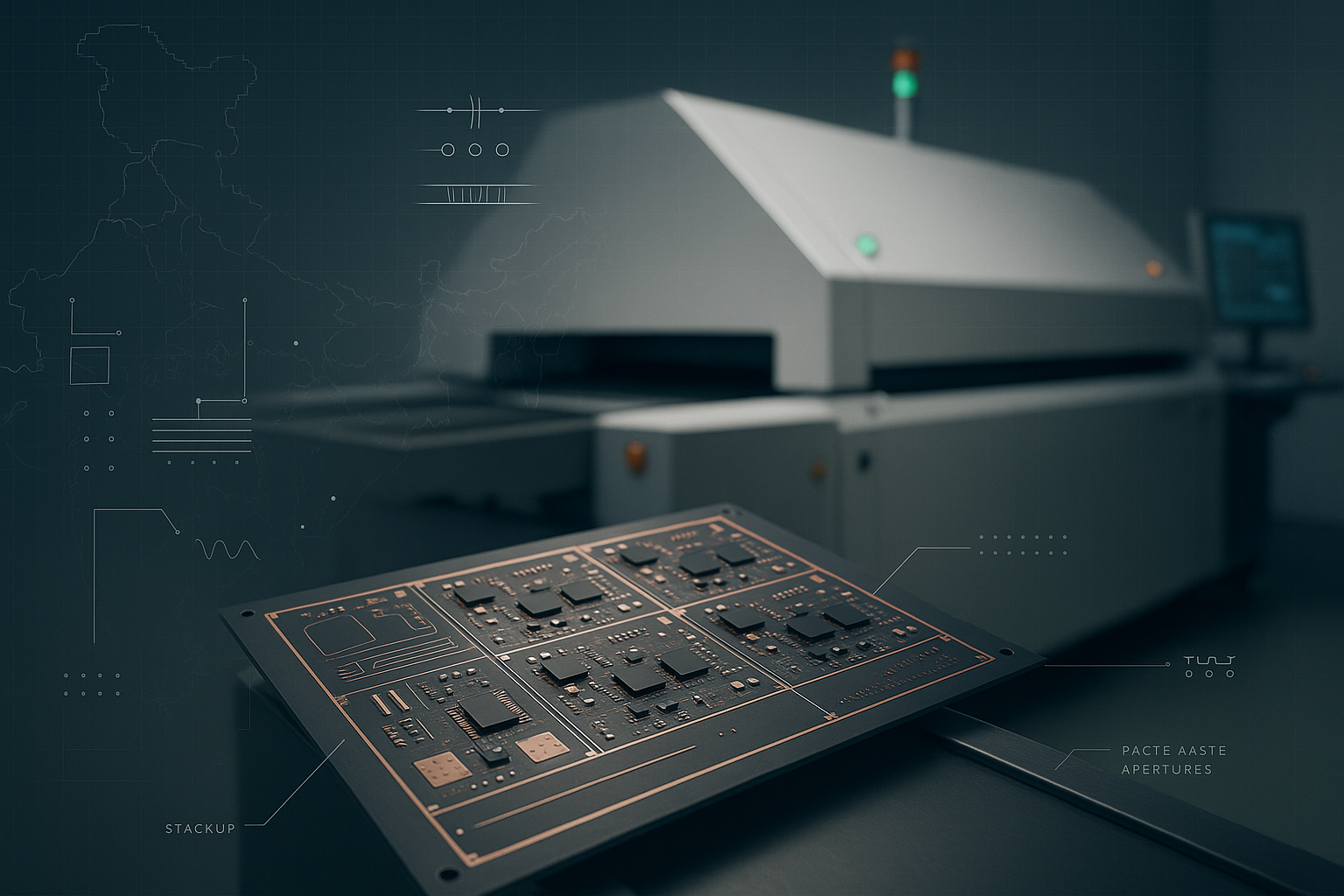
PCBs with more than 2 layers of conductive material are called multilayer PCBs. They are constructed like a sandwich with multiple layers of copper foils as conductive material that are bonded through high heat and pressure. Insulating sheets are present between these layers for protection.
Usually, outer layers are meant for placing the components while the inner layers that are coated with copper are used for routing the connections. Apart from these, the layers are bound together through prepregs created from glass fibres saturated with epoxy resin.
Benefits of Multilayer PCB
Check out some main benefits of multilayer PCBs:
- They facilitate complex circuit designs for sophisticated electrical devices like smartphones, laptops, aerospace systems, etc., using multilayer PCBs.
- Multilayer PCBs are comparatively smaller and lighter. This makes it ideal for electronic devices that feature compactness.
- Manufacturers need not connect multiple separate PCBs. Therefore, the creation process will be more simple.
- Unlike other forms of PCBs, the unique properties of multilayer PCBs improve the speed and efficiency of devices.
- When it comes to the manufacturing process, multilayer PCBs may provide significant benefits. Sometimes multiple functions can be integrated into a single multilayer board. That means manufacturers can save the time and effort spent in manufacturing separate PCBs.
Disadvantages of Multilayer PCBs
Just like a coin having both sides, multilayer PCBs have their own demerits. Some of them are as follows:
- Multilayer PCBs are comparatively more expensive to design and manufacture.
- Processes like arranging the interconnections and precise signal routing during manufacturing require intense technical expertise. Even a small mistake in the manufacturing process can make the entire PCB useless.
- The internal connections in multilayer PCBs are not visible. As a result, it is more difficult to identify and fix problems.
- Some specialised equipment and materials are required to create Multilayer PCBs. A limited availability of such materials affects the production of multilayer PCBs.

Why Are Multi-layer PCBs Designed with an Even Number of Layers?
There are several reasons as to why multilayer PCBs are designed with an even number of layers. Here are some of them:
- Multilayer PCBs are created through a process of lamination. An even number of layers ensures a symmetrical distribution of material on both sides of the central core to avoid the chances of warp.
- The balanced structure of the layer ensures that all sides of the board have equal access to signal transmission and this improves the signal quality of the device.
- The symmetrical structure of multilayer PCBs minimises the chances of manufacturing defects like scratches, PCB etching errors, etc.
- Multilayer PCB manufacturing often involves processes optimised for handling an even number of layers. Adding an extra layer may increase the complexity of manufacturing and add up to the costs.
- Even-layered PCBs are known to withstand thermal pressures during the manufacturing process in a better manner.
PCB Layout Rules
As mentioned earlier, even a minor mistake made during the creation of PCB can have severe consequences. That's why it is important to abide by certain rules and standards while manufacturing PCBs. Here are some of them:
1. Balanced Component Placement
Most devices have some PCB components that are to be placed in specific locations. First of all, lock such must-have components in the required location during the PCB fabrication process. Then, try to place the rest of the components in a balanced structure avoiding any kind of layer transitions.
2. Proper Signal Integrity
It is always better to keep the distance between signal lines and return paths to the minimum to ensure signal integrity. Conduct proper tests to detect and avoid crossing areas of the circuit with analogue traces.
3. Placement of Power and Ground Planes
Power and ground planes should be placed symmetrically. This way, electromagnetic interference could be reduced to a great extent.
4. Layer Stacking
As mentioned before, even the number of layers always works better. It has a lot of benefits from minimisation of warping to signal reliability. Also, make sure that the PCB goes through a rigorous process of Design for Manufacturability (DFM) check for approval that it is viable and cost-efficient.
Final Thoughts
To wrap it up, PCB layers are the base upon which many electrical devices are built. The unscientific assembly of PCBs without proper knowledge may cause significant consequences, both in terms of cost and quality. From the process of PCB fabrication to assembly, each step must be properly monitored by experts. Last but not least, test to verify that the PCB design meets all requirements and standards.