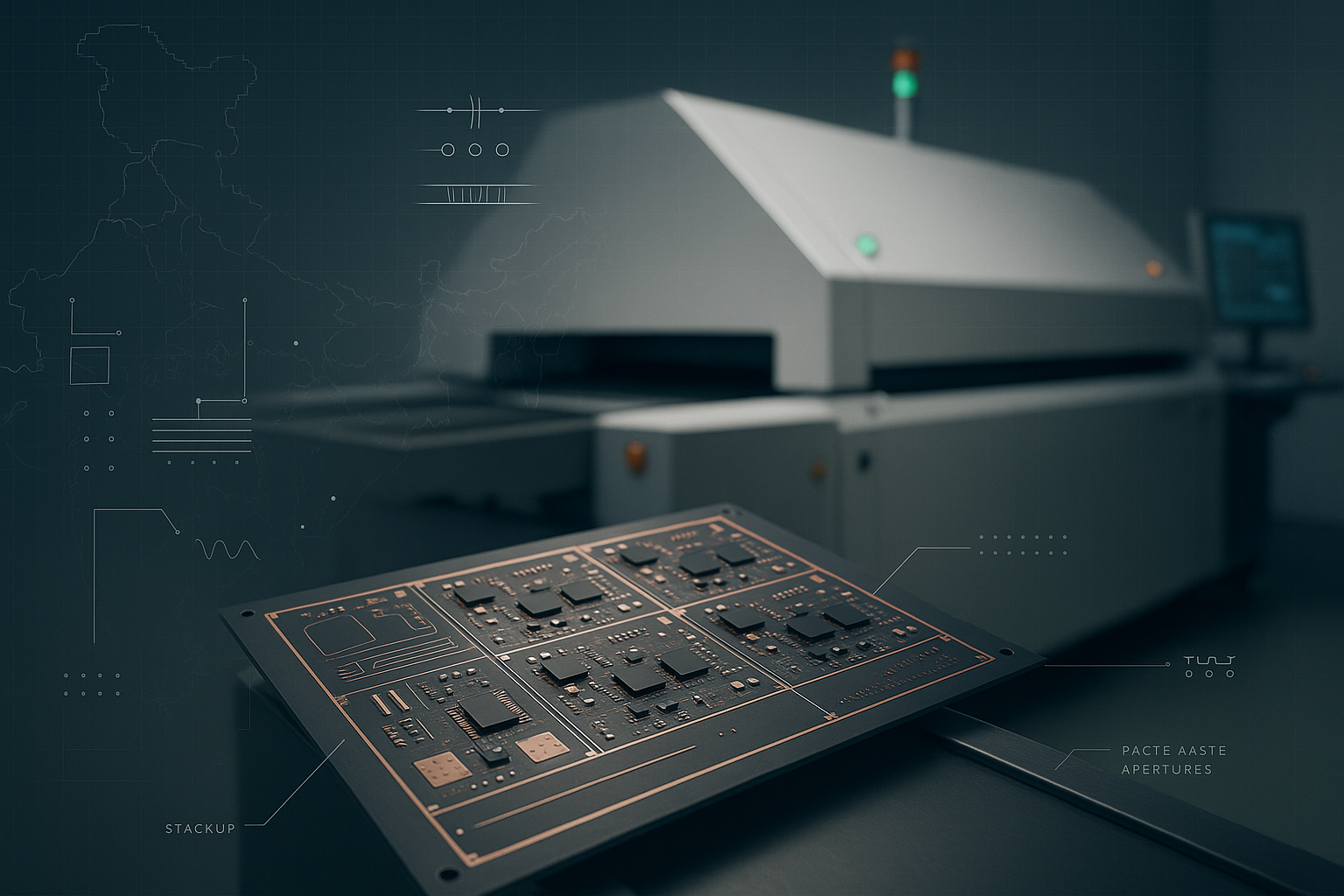
As the entire PCB market is switching to solutions with higher density and precision, the demand for ceramic PCBs is rising like never before. It is a type of PCB that uses ceramic materials as a base. Ceramic PCBs have had a strong presence in the electronic industry for years due to their high thermal conductivity and chemical resistance.
This blog will provide a comprehensive picture of ceramic PCBs, discussing what it is, the types of ceramic PCBs, the manufacturing process, and several guidelines.
Key Highlights
- A ceramic PCB is a type of printed circuit board that is made up of ceramic materials.
- The three main types of ceramic PCBs are High-Temperature Ceramic PCBs, Low-Temperature Ceramic PCBs, and Thick-film Ceramic PCBs.
- Some of the main advantages of ceramic PCBs are superior thermal management, mechanical strength, low dielectric constant, and miniaturisation.
- The manufacturing process of ceramic PCBs goes through several stages like raw material selection, ceramic powder preparation, screen printing, lamination, sintering, and quality control
- As compared to other boards, ceramic PCBs are well-known for its higher thermal conductivity and low dielectric constant.
- Ceramic PCBs are used in many sectors like medical, communication, defence, automotive, aerospace, etc.
What is a Ceramic PCB?
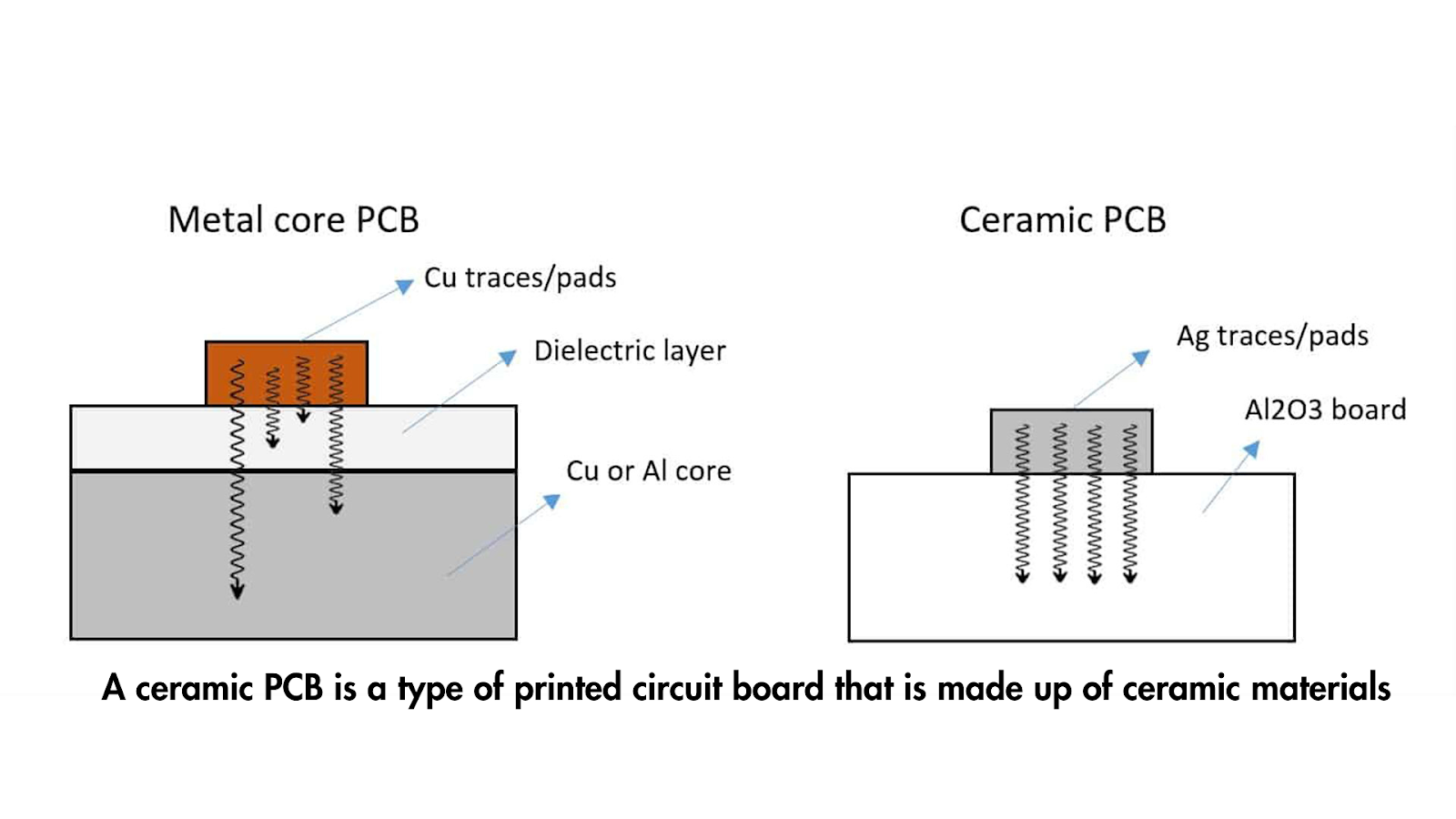
As mentioned before, a ceramic PCB is a type of printed circuit board that is made up of ceramic materials. Usually, the base of PCBs is made of traditional fibreglass or epoxy resin. But when it comes to ceramic PCBs, the base is made of a protective layer of ceramic material and a metal component.
Such ceramic materials like alumina (Al2O3) and aluminium nitride (AlN) have higher thermal conductivity to safeguard the PCB during high-temperature processes and lower thermal resistance of typically within 0.31 K/W. On top of that, since ceramic PCBs are baked up to 1000°C in a nitrogen atmosphere after coating the base with copper, oxidation is prevented. This makes them a perfect choice for industries like space, military, aerospace, etc., where devices are subjected to harsh environments.
Types of Ceramic PCBs
There are several types of ceramic PCBs based on various factors. Have a look at some of them:
1) High-Temperature Co-fired Ceramic (HTCC) PCBs
HTCC PCBs are a kind of ceramic PCBs that are made up of alumina (Al2O3) or aluminium nitride (AlN) materials. As the name suggests, they are heated at high temperatures, typically above 1600°C to bond the ceramic and metal layers. They are specifically known for excellent thermal conductivity and high-temperature applications which could be really useful for sectors like aerospace, automotive, etc.
2) Low-Temperature Co-fired Ceramic (LTCC) PCBs
LTCCs are composed of a glass-ceramic composite material that can be fired only at lower temperatures (approximately 900°C). The best part about LTCC is that they are adaptable to low-resistance metals like silver and copper for conductive traces. These types of PCBs are mainly used for multilayer PCBs that demand high-frequency performance and low warpage.
3) Thick-film ceramic PCBs
Just like HTCCs, thick-film ceramic PCBs are mainly composed of alumina or aluminium nitride (85% -96%). Since their base is coated with any metal like gold, silver, or copper, they are mainly used in cases where there are risks of oxidation and require high thermal conductivity.
Advantages of Ceramic PCBs
Ceramic PCBs are gaining immense popularity in the industry due to the cool set of benefits that they offer. Here are some of them:
1) Thermal Management
What makes ceramic PCBs unique is their high thermal conductivity, which is closer to silicon. This property shields the PCB components from damages caused due to overheating as it can effectively dissipate the heat.
2) Mechanical Strength and Durability
The materials used to create ceramic PCBs like alumina are well-known for higher mechanical strength. It prepares the PCBs to withstand harsh environments and voltages without causing any breakdowns. Apart from that, ceramic PCBs have a higher degree of chemical resistance which makes it protect the material from environmental degradations. As a result, the lifetime of devices will be longer.
3) Low Dielectric Constant
Yet another highlighting benefit of ceramic PCBs is their low dielectric constant which makes it easier for electric fields to penetrate. Typically, the dielectric constant ranges from 4 to 10. It helps devices to transmit signals instantly and is, therefore, suitable for those requiring high-frequency PCB signal transmission.
4) Miniaturisation
The manufacturing process of ceramic PCBs itself is designed to facilitate a tighter component placement. Due to the usage of thinner dielectric layers, it helps manufacturers to cut the size of the devices.
Manufacturing Process of Ceramic PCB
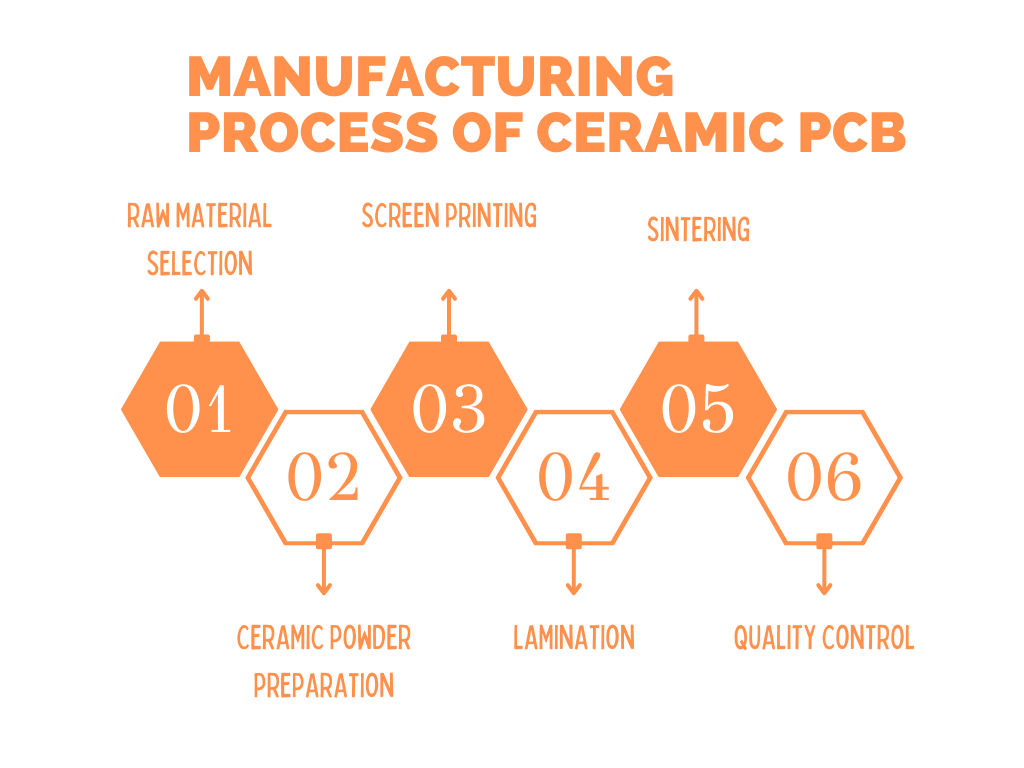
The manufacturing of ceramic PCBs requires various steps. Check out them:
1) Raw Material Selection
First of all, manufacturers need to acquire top-quality raw materials. The raw materials required basically depend on the usage of the ceramic PCB. For instance, Aluminium Oxide may be perfect for devices that demand high electric insulation while Silicon Carbide is suitable for situations when components are subjected to high temperatures during manufacturing. Apart from the base materials, conductive pastes with metallic components like silver or gold are also used.
2) Ceramic Powder Preparation
All the components are combined together through a grinding process to create ceramic powder. This powder is rolled out through organic binders to get a fine mixture called green sheets, which serves as the substrate of the board.
3) Screen Printing
A thick film of a metal like gold or silver is printed on the green sheet surface to devise the conductive pathways for the PCB. Make sure that this process is done in the presence of expert professionals as even a minor deviation can make the entire PCB etching useless.
4) Lamination
Now, the green sheet is arranged layer upon layer with precise alignment to ensure that circuit pathways are in the right manner. The stacked green sheets are laminated under high pressure, around 20-30 MPa to eliminate any air gaps between the layers. After that, it is cut into the required size.
5) Sintering
The ceramic pieces are heated carefully in a controlled environment. As a result, the ceramic layers and conductors turn into a solid structure. Moreover, the organic binding process remains completely wiped out. The entire process takes up to 48 hours to complete.
6) Quality Control and Testing
After the process, the entire PCB undergoes a series of quality tests to ensure that the board is capable enough to work reliably in harsh environments. Various factors like thermal resistance, electronic performance, etc. are tested.
Comparison Of Ceramic PCB with Other PCB Materials
For a better understanding, have a look at how ceramic PCB performs as compared to its alternatives.
1) Ceramic PCB VS Teflon PCB
Since Ceramic PCB manufacturing goes through higher temperatures, the materials are limited and production incurs heavier costs. On the other hand, teflon PCB is less brittle as compared to ceramic boards which makes it easier for manufacturing. However, the problem is that teflon boards have a higher coefficient for thermal expansion which is a serious concern for manufacturers focusing on the reliability of the device.
2) Ceramic PCB VS FR4 PCB
When it comes to thermal conductivity, ceramic PCB has a clear-cut edge over FR4 PCB. Therefore, if you are considering using boards for devices that go through many heating processes, ceramic PCBs are the best choice.
Most probably, FR4 PCBs are made of copper and steel alloy. Even though they provide stiffness, materials like copper might increase the production cost.
3) Ceramic PCB VS MCPCB
The first difference between ceramic PCBs and metallic-core PCBs is an insulative layer. The substrate formed during the manufacturing of ceramic PCBs acts as an insulative layer. However, MCPCBs require an additional insulation layer between the metal core and the copper traces after the process.
As the name suggests, the base of ceramic PCBs is made of ceramic materials while MCPCBs usually use a metal core like aluminium to cut the costs.
4) Ceramic PCB VS HDI PCB
HDI PCBs require more trained professionals throughout the process as they have much more interconnecting density and higher wiring compared to other PCBs. Even though this high interconnecting density contributes to the thermal management properties, it is not at all close to the superior thermal advantages offered by ceramic PCBs.
Design and Fabrication Considerations
Regular checking and performance tests are required during each stage of the manufacturing process to ensure the efficiency of ceramic PCB. Here are some simple guidelines for that:
- Solder masks on ceramic PCBs must be thicker as the material is more porous. Consider using more protective surface finishes like ENIG PCB(Electroless Nickel Immersion Gold).
- Each layer of ceramic multilayer PCBs must be manufactured individually with the presence of expert professionals.
- Since ceramic PCBs are more brittle, vias must be placed with proper space in between.
- Specialised equipment is required in the PCB fabrication process to prevent damage to the material.
Applications and Industries
Ceramic PCBs are widely used in many industries due to their versatile features. Check out some sectors where they are most applicable.
1) Aerospace and Defence Systems
The key highlight of ceramic PCBs is their high thermal conductivity, which makes the devices perform perfectly in harsh environments. This is particularly useful for aerospace and defence sectors where equipment like missile guidance systems are working under extreme temperature conditions. Moreover, the low dielectric constant property improves the signal performance of the device which makes it perfect for RF PCB radar systems and communication equipment.
2) Automotive and Transportation
The thermal conductivity property of ceramic PCBs helps automotive devices dissipate heat from inverters and motor drives. Its ability to withstand harsh environments makes it well-suited for power systems, sensor modules, lighting, etc.
3) Medical and Healthcare
Since ceramic PCBs protect the components from degradations, it is a common choice for equipment like surgical instruments, where performance reliability is crucial. Apart from that, they are also used for implantable medical devices due to the environment-friendly nature of ceramic materials.
Conclusion
The entire area of ceramic PCB is evolving with ongoing research to improve mechanical strength and reliability. As a result, more and more industries are exploring the opportunities behind them each day. In a nutshell, the future of ceramic PCBs looks brighter than ever before.