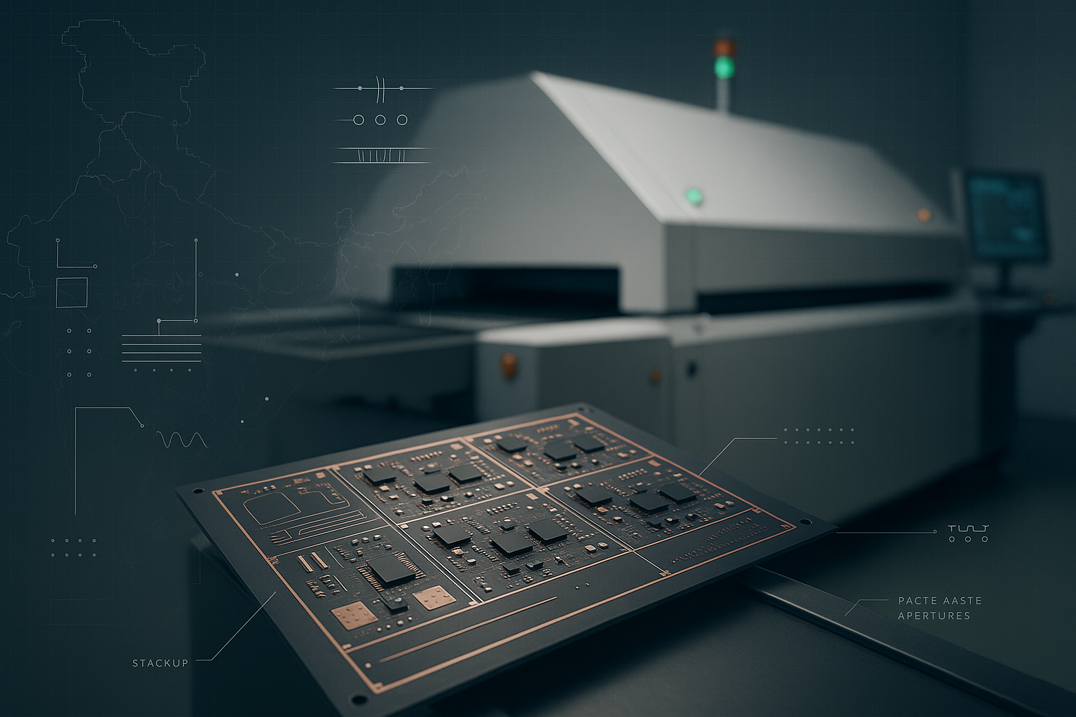
A ball grid array (BGA) is a type of surface-mount packaging for integrated circuits. It adds more connections to the chip without using pins and lines. On the bottom of the device, they use a grid of very small solder balls instead. The integrated circuit and the printed circuit board (PCB) are linked by solder balls.
One of the most striking features of BGA packages is that they work better with electricity and heat. Low inductance and resistance are caused by the short lengths of the leads. It makes the signal stronger and moves info faster. PCB layers play a crucial role in the design and functionality of BGA packages, allowing for complex routing and signal isolation.
Another good thing about the solder balls is that they make it easier for heat to escape, which is very important for high-performance uses. It's also good that BGA packages are small because they help the trend of tech getting smaller. This article will discuss in-depth about BGAs, including what it is, types, inspection methods, and industry trends.
Key Highlights
- A ball grid array (BGA) is a type of surface-mount packaging for integrated circuits.
- There are 3 main types of BGAs: Plastic Ball-Grid Arrays, Ceramic Ball-Grid Arrays, and Tape Ball-Grid Arrays.
- Some of the main advantages of BGA technologies are high-speed efficiency, surplus pins, and effective heat dissipation while the major concerns are high costs, chances of errors, and need for close inspection.
- Electrical testing is an important part of inspecting Ball Grid Array (BGA) packages to make sure that electrical devices work well and are reliable.
- Ball-Grid Arrays are mainly used in devices like smartphones, laptops, and high-speed electric circuits.
Definition and Overview
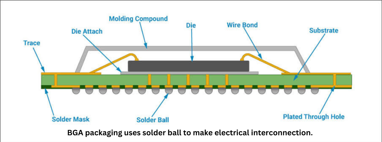
Ball Grid Array has a grid of small solder balls on the bottom of an integrated circuit. BGA packaging is important for modern electronics. They are mainly famous as they improve speed and reliability.
During PCB assembly, BGA technology offers a number of benefits. It has a higher number of solder balls, which makes forging more connections possible. It improves both the electrical and thermal performance.
When lead lengths are cut down, inductance and resistance go down. That’s why signal integrity and data transfer speeds improve a lot. The bigger contact area of the solder balls also makes it easier for heat to escape. It is important for high-performance applications.
BGA packages also support the move in electronics toward smaller sizes. It makes them perfect for devices that are small.
But there are some problems with BGA technology. It's hard to check the solder joints because they are under the package. Visual inspections done the old-fashioned way don't work. That’s why more advanced methods like X-ray inspection are needed.
Also, rework and repair of BGA packages are harder because the solder balls are covered. Hence, special tools and knowledge are required to do them. Also the parts in PCB layers are needed to be lined up correctly and soldered properly during assembly. These are very important to avoid problems like shorts or leaks. The selection and placement of PCB components are critical factors in maintaining signal integrity in BGA packages.
History and Evolution OF BGA
During its development, Ball Grid Array technology was a big step forward fro, Pin Grid Arrays (PGAs) because the pins on PGAs stuck out from the bottom. Hence, they could bend and become out of line, which caused connectivity problems.
To get around these problems, BGA was created. It uses a grid of solder balls on the bottom of the box to make connections. This PCB layout helps the links to line up properly. It puts less stress on the links mechanically, and assists to make more connections.
PCB gold fingers are often used in BGA packages to ensure reliable connections and minimise signal loss at board edges.
A lot of the progress made in BGA technology has been in making soldering better and more reliable. One big step forward is the creation of lead-free solder balls. These are better for the environment and follow international rules.
More reliable and solid BGA connections have been made possible by better soldering methods, like reflow soldering. It has resolved issues like voids and incomplete solder joints. BGA technology has also grown to include different types that are better for different uses.
Micro BGA (µBGA) packages, for example, are made for very small devices. They offer a lot of interconnects in a small box. The development of multilayer PCB technology has greatly enhanced the capabilities of BGA packages, allowing for more complex designs and better performance.
Thermally Enhanced BGA (TEBGA) packages are perfect for high-power uses. Because they are made with materials and designs that help them get rid of heat better.
Plastic BGA (PBGA) and Tape BGA (TBGA) are both cost-effective in nature. Encapsulated materials are used in these BGAs.
Types of BGA Packages
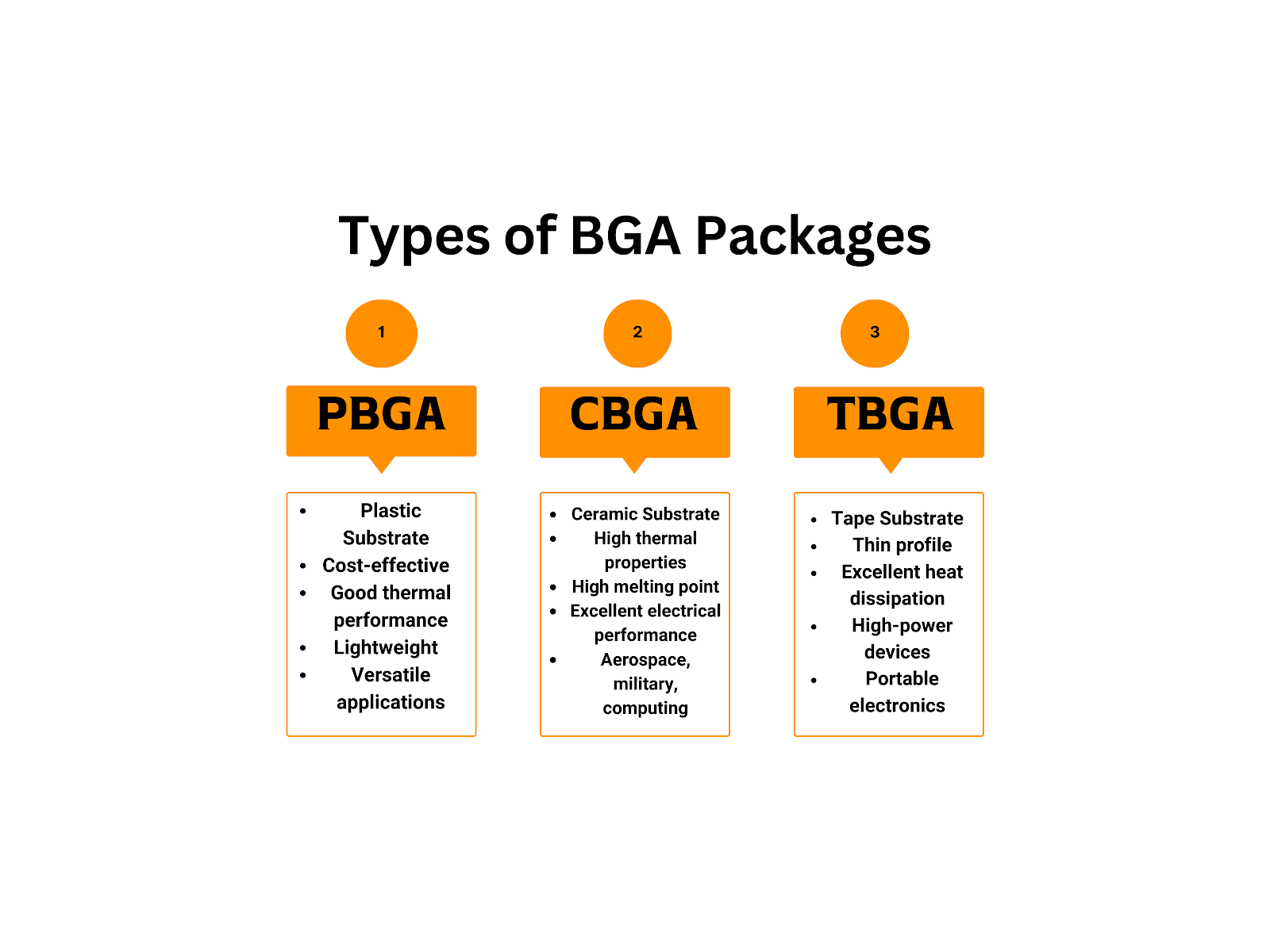
Three kinds of BGA packages are on the market—PBGA, CBGA, and TBGA. Every one of them has its advantages and its own characteristics. Knowing these kinds will enable manufacturers to select the ideal BGA package for their electronic devices.
1. Plastic Ball Grid Array (PBGA)
PBGA is known for being flexible and low-cost. In this package, the integrated circuit is housed in a plastic substrate. Then, at the bottom, solder balls are arranged in a grid design. The links between the IC and the PCB work well with this setup.
Features:
PBGA packages are made with a plastic base that makes them very light. It makes them perfect for many uses. The solder balls on the bottom make a strong connection that makes the gadget work better overall.
Advantages:
The main benefits of PBGA are that it is cheaper to make because it is made from plastic, it has good thermal performance that helps heat escape, and it has excellent electrical qualities that make sure it works reliably. These things help explain why PBGA is used so widely in many fields. The design of PCB pad structures is crucial in BGA packages to maintain consistent impedance and minimise signal reflections.
Applications:
PBGA packages are used a lot in consumer gadgets, car systems, and many other industrial settings. They are extremely reliable and inexpensive options. That’s why manufacturers choose these BGA types for various electronic products.
2. Ceramic Ball Grid Array (CBGA)
CBGA is made of ceramic material. It makes them stand out for better thermal and mechanical features. Since the ceramic material allows for a higher melting point, CBGAs are perfect for uses that need to work at high temperatures.
Features:
The ceramic base in CBGA packages is very good at keeping temperatures stable and being strong. Because clay has a high melting point, the package can withstand very high or very low temperatures without breaking down. The use of a PCB stencil is often necessary for precise application of solder paste in BGA assembly, especially for fine-pitch packages.
Benefits:
The ceramic base in CBGA packages improves the electrical performance and dependability, especially when the package is exposed to high temperatures. The ceramic material is also resistant to water and other natural factors, so it will last for a long time.
Applications:
CBGA packages are often used in high-end computers, defence systems, and aerospace where reliability, durability, and control of heat are important. This kind of tough climate is good for ceramic PCB because it is strong.
3. Tape Ball Grid Array (TBGA)
This type of chip is made for uses that need strong core materials in thin, light packages. Because it is made on a tape base, this type of BGA has a thinner profile than other types.
Features:
TBGA packages have a tape base that helps them be thin and light. The strong core materials used in TBGA make the package last longer and work better.
Advantages:
TBGA's main benefits are good heat dissipation, which is important for high-power devices, and stable electrical connectivity, which is made possible by the high-quality core materials. Because of these qualities, TBGA can be used in situations that need strong thermal control and a small design.
Applications:
TBGA packages are often used in portable electronics like smartphones and tablets, where managing room and heat is very important. TBGA is perfect for these high-density, high-performance uses because it has a thin shape and quickly gets rid of heat.
Advantages and Disadvantages of BGA
BGA technology has many advantages that make it a good choice for high-tech computer uses. On the other hand, it also brings problems. Manufacturers must find a balance between these pros and cons in order to use BGA packages effectively in their goods.
Advantages of BGA Technology
- High-speed efficiency is one of the main benefits. Since the electrical lines inside a BGA package are short, inductance and resistance are lower. This makes the signal stronger and speeds up data transfer. This feature is especially helpful for high-frequency uses where clear signals are very important. HDI PCB (High Density Interconnect) technology is often employed in BGA designs to reduce signal path lengths and improve overall performance.
- One more big benefit of BGA packages is that they have a lot of pins. Arrays of solder balls make it possible for more connections to be made in a smaller space than with regular pin grid arrays (PGAs) or dual in-line packages (DIPs). This higher density helps make electronics smaller. It allows for more complex and space-saving designs without sacrificing usefulness.
- Another great thing about BGA technology is that it better moves heat around. The bigger surface area of the solder balls makes them better at conducting heat. It means that heat moves more quickly from the integrated circuit to the printed circuit board. This feature is very important for high-performance devices that produce a lot of heat, keeping them stable and avoiding damage from heat.
Disadvantages of BGA Technology
Even though BGA technology has some benefits, it also has some problems.
- Solder joints are more likely to break, which is a big problem. The solder balls in BGA packages can be stressed by mechanical forces. It especially happens in places where there is a lot of temperature change or mechanical shaking. These situations can cause the solder joints to crack, which could cause the link to fail.
- Another problem is that BGA packages need to be inspected and tested. The solder balls are on the bottom of the package. That’s why it is hard to see the solder joints.
- The manufacturing process of BGA assembly is more complicated and expensive. Since it needs more advanced checking methods like X-ray imaging to find flaws. It can also be hard to make circuits with BGA packages. Because the parts need to be precisely aligned and soldered.
- If something isn't lined up right during the building process, it can cause problems like shorts or openings that affect how well the device works and how reliable it is.
- BGA packages are also harder to update and fix than other types of packages, and they often need special tools and skills to do so.
- Last but not least, one big problem is that soldering and checking require expensive tools. The unique tools and methods needed to work with BGA packages raise the overall cost of production, which makes them harder for low-budget projects or smaller makers to use.
Inspection and Testing OF Ball Grid Array
Electrical testing is an important part of inspecting Ball Grid Array (BGA) packages to make sure that electrical devices work well and are reliable. This test is mostly about finding open circuit and short circuit problems, which often happen during the making process.
Open circuits happen when there is a break in the electrical path that stops current flow. Short circuits happen when conductors join without meaning to, letting current flow in the wrong direction.
1. Identifying Open Circuit Defects
There are many things that can go wrong with BGA packages. It can cause open circuit flaws, such as bad soldering, misalignment, or damage to the solder balls.
Electrical testing can help find these problems. By checking the continuity of the electrical lines, producers can resolve this issue. If a connection is lost, it means there is an open circuit, which can make the gadget less useful.
2. Identifying Short Circuit Defects
When solder balls bridge nearby connections, making unintended electrical paths, short circuits can happen. By measuring the resistance between the connections, electrical tests can find these shorts.
A resistance number that is lower than expected usually means that there is a short circuit. It is important to find and fix these problems right away to keep the electronic gadget from breaking down or malfunctioning.
3. Boundary Scan Inspection
One way to find component opens and shorts in BGA packages is to use boundary scan analysis. With this method, producers can check each solder joint on the boundary connection for problems with connectivity.
How It Works?
- A boundary scan description language (BSDL) file and a test access port (TAP) are used to control and see the state of each pin.
- Checks for continuity and good connections to make sure that solder joints are strong.
- Finds opens and shorts at the PCB component level, making sure the gadget works reliably.
- Taconic PCB materials are sometimes used in high-performance BGA designs for their excellent electrical and thermal properties.
Advantages
- Non-intrusive way that doesn't need to touch the solder joints directly.
- Able to test circuits with a lot of pins that are very complicated.
- Gives detailed information on where flaws are and what kind they are.
4. Automated X-ray Inspection
Another important way to check solder joints in BGA packages is with automated X-ray inspection (AXI). With this method, solder joints under components can be inspected, showing flaws like gaps and bubbles that were not visible before.
How It Works?
- X-rays are used to get inside the BGA package and take clear pictures of the solder joints.
- Look at the pictures to find problems like holes, bubbles, and not enough solder.
- The checking process is more accurate and faster when it uses automated systems.
Advantages:
- Offers a way to check secret solder joints without damaging them.
- Can find flaws that regular checking methods can't see.
- Makes BGA systems more reliable and better overall.
Importance of Inspection and Testing
There are several grounds why BGA packages should be examined and tested. Initially, they identify issues that could break electronic equipment, therefore ensuring that they function and are dependable.
Early identification and resolution of issues like short circuits, open circuits, and solder joint flaws reduces the likelihood that defective products will reach the market.
Electronics items are also improved in terms of performance and quality by thorough testing and inspection. These factors make sure every component functions well. It enables manufacturers to produce goods that satisfy customers and high standards.
It is particularly crucial for applications in safety-critical industries. Industries like aviation, cars, and medical devices are dependable on safety. That’s why these tests are required. With time, good testing and inspection also contribute to reduced production costs.
Recalls, repairs, and expensive guarantee claims can be avoided by businesses that identify and resolve issues fast. In addition to improving product quality, using inspection techniques increases production efficiency.
Elimination of Defects in BGA Packages
Getting rid of flaws in BGA packages is important for keeping the quality and dependability of electronics high. Companies can make sure their products work well and are reliable by getting rid of all flaws properly. These products should meet industry standards and customer expectations.
a) Process of Eliminating Defects
- Detaching Components
- When problems are found, removing the faulty BGA chip from the PCB is often the first thing that needs to be done.
- To keep from damaging the board or nearby parts, this method needs to be handled carefully.
- Hot air rework machines and other specialised tools are used to melt the solder balls, which makes it safe to remove the BGA package.
- BGA Rework
- Cleaning the PCB and the BGA package to get rid of any leftover solder is part of BGA rework.
- The surface is ready to be soldered again after it has been cleaned. The BGA package is then realigned with the PCB using exact alignment tools to make sure it is in the right place.
- Reflow soldering methods are used to reconnect the BGA package, making sure that the connection is strong and stable.
- Localised Heating
- By heating only certain parts of the BGA chip, solder joints can be fixed without taking the whole part out.
- This method can be used to fix problems like cold joints or not enough glue. Using special tools, controlled heat is given to the broken area.
- This reflows the solder and fixes the problem. This method lowers the chance of hurting nearby parts and the amount of work that needs to be redone.
b) Importance of Eliminating Defects
Ball Grid Array (BGA) packages must be free of defects if electronic devices are to function properly and last a long period. Open circuits, short circuits, and intermittent connections are among the issues that can arise from solder joint issues and reduce the usefulness of the entire system.
Early correction of these defects is necessary. In the manufacturing process, it helps prevent costly repairs or recalls from damaging the brand's reputation.
Moreover, quality control of the BGA assemblies ensures safety. Particularly in industries like medical, automotive, and aerospace electronics where device dependability is crucial, quality control is essential.
Applications and Industry Trends
BGA technology is very important in many fields. It includes high-speed electronic systems, laptops, and cell phones. New types are being made all the time in BGA technology right now. With these changes, BGA technology will be able to keep up with the needs of current electronics.
Applications of BGA Technology
1) Laptops
Because it has a high pin density and is small, BGA technology is used a lot in laptops. This is because it helps current portable computers get smaller and faster. Since laptop electronics are so complicated, BGA packages are needed to make sure that heat is properly dissipated and that electrical connections are stable.
2) Mobile Devices
BGA packages are small enough and have a lot of connections to work well in mobile devices like smartphones and tablets. BGAs are perfect for the tightly packed parts in mobile electronics because they can handle high data rates and handle heat well, t
3) High-Speed Electronic Circuits
BGA technology is very important for high-speed computer circuits, like those in data centres and networking gear. Due to short electrical paths, they improve speed and reduce signal loss. It makes them good for uses that need to send signals in high frequency PCB.
Industry Trends in BGA Technology
People in the business are making new kinds of BGA packages that are better suited for certain uses. Micro BGA (µBGA) packages, on the other hand, are made for very small devices.
Along with that, Thermally Enhanced BGA (TEBGA) packages are intended to handle high-power applications with better heat dissipation. These new ideas meet the changing needs of various industries, which makes sure that BGA technology stays useful.
1) Improvements in Inspection and Testing Methods
Inspection and testing methods are getting better, which makes BGA packages much more reliable. More advanced methods like boundary scan inspection and automated X-ray inspection can now find flaws more easily and make sure that high-quality parts are made. These changes help manufacturers keep a close eye on quality and meet standards in the business.
2) Enhanced Thermal Management
Better thermal control in BGA packages has become very important as the power density of electronics has grown. New materials and designs are making BGA packages better. With these updates, getting rid of heat becomes smooth. It keeps gadgets working well without getting too hot.
3) Integration with Advanced Packaging Technologies
There are two advanced packaging solutions— System-in-Package (SiP) and Multi-Chip Module (MCM). They are being used more and more with BGA technology. This integration makes it possible for designs to be more complicated and small, which supports the trend in electronics toward smaller sizes and better performance.
Conclusion
Electronics of today heavily rely on ball grid array technology. For it offers improved heat conduction, a high pin density, and steady high-speed performance. Its applications are so numerous and include high-speed computer circuits, laptops, and mobile devices. Furthermore, since new BGA types are developed continuously and testing and checking techniques improve continuously. Such is its significance, as demonstrated.
BGA technology is probably going to evolve much farther in the future. It will include temperature control and combining with more sophisticated packaging technologies. Still, issues like guaranteeing defect-free products and controlling production costs will need to be addressed if electronic manufacturing is to continue to be a major force.